 |
■研究開発経歴 / R&D History ・ 経歴 / History ・野鳥撮影 / Bird Photograph |
トレンチセル / Trench Cell
■西澤潤一メダル受賞に当たって ■トレンチキャパシタセルとは ■発明のきっかけ ■特許出願 ■試作着手と動作成功s ■IEDM:58件の優秀発表に選定 ■製品化開発を覆った暗雲 ■西澤潤一メダル受賞 ■終わりに |
|
[主要更新] '16.11.14: 本サイト再構築 '09.11.26: 「トレンチキャパシタ」分離 '05-6:原www.suna.cc開設 |
筆者は2006年6月に小柳光正・東北大学教授、伊藤清男・日立製作所フェローとともに、米国電気電子学会(IEEE)が2002年に創設した半導体材料・デバイス分野で優れた業績を挙げた研究者を表彰する『西沢潤一メダル』を授与された。高集積DRAMに不可欠な2種類のセル構造の一方、トレンチ(溝堀り)キャパシタ(容量)を開発した功績が評価されたもので、日本人として初の受賞であった。小柳教授は他方のスタックキャパシタ、伊藤フェローはメモリアレー構成、3人とも日立中央研究所時代の業績で授与された。筆者は過去にもこの発明で、IEEEポール・ラパポート賞、IEEEクレド・ブルネッティ賞、IEEEフェロー、日本電子情報通信学会フェロー、東京都発明研究功労者表彰等を受賞している。ここにトレンチキャパシタの発案、特許出願から共同受賞者ともに進めた製品開発経緯を記したい。
また、この受賞に当たって、2006年6月「半導体シニヤ協会機関誌」より、トレンチキャパシタ発明と開発の経緯について寄稿の依頼を受けた。本文は同誌2006年10月号とその次号に掲載された内容をまとめたものである。また、拙書「技術者のための特許事始めー半導体技術を中心として」にも簡単な経緯を述べた。
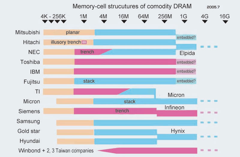
トレンチキャパシタセル(略してトレンチセル)とは、1トランジスタ+1キャパシタで構成されるダイナミック・ランダム・アクセス・メモリ(dynamic-random-access memory, DRAM) のメモリセルのキャパシタを、シリコン基板の中に掘り込んだ溝(トレンチ)の中に形成するものである。平面面積を増大することなく大容量のキャパシタが形成できるので、スタックと並んで現在のDRAMに不可欠のセルとなっている。下図に2005年時点におけるDRAM製品でのトレンチとスタックの採用状況を示す。

●鉱石ラジオからはじまる
私のルーツは小学校の工作で格闘した鉱石ラジオである。エナメル線をボビンに巻き、コイルの一部を紙やすりでこすって銅線をむき出しにして接点をつくる。工作と絵は得意であった。でも音が聞こえてこない。ものの本を読むと鉱石が悪いことが多いとあったので、いろいろと調べた。鉱石がロッシェル塩でできていること、周波数とは、同調とは、検波とは、訳もわからず鵜呑みの知識が増えていった。
中学、高校とこれがエスカレートし、趣味となった。真空管を4本使った並四受信機に始まって、ダブルスーパーヘテロダイン短波受信機まで及んだ。しょっちゅう秋葉原に通い、米軍払い下げの送受信機の見事な造りに感動したりした。当時はアマチュア無線全盛のころで、短波送信管807を使って送信機も作った。大学受験で気持ちのゆとりもなく、あのシャーシャーという雑音だらけの中からかすかな音声を拾うアマチュア無線通信に違和感があったのも確かで、結局免許はとらずにコールサインは貰いじまい。もらっていたらJA1何がしかでビンテージものとして尊敬されているだろう。
大学以降は無線からオーディに移った。通常使わない電力真空管などを選び、これとインピーダンスマッチングするトランスを苦労して探し、世界で唯一のメインアンプなどと悦にいっていた。真空管は最大定格で使うものと思っていたのが間違いで、まもなくこの真空管は過負荷でおしゃかになった。その後トランジスタアンプに移り、造り上げた台数は10を超えたが、今残っているのは1台のみ。
●西澤先生に投げかけられたトラウマ
東北大学での卒業研究・修士研究では半導体を選んだ。不遜なことに、造り続けた送受信機やアンプの回路はどうも“底が浅く”て研究対象として考えられず、対極にあるプロセスへと方向を定めた。趣味と仕事は別にしたいという思いもあった。回路に向かっていたら違った研究人生になっていただろう。このとき師事した西澤先生の背中で語る教えは強烈で今でもトラウマになっている。「論文は読むな。他人と同じことはするな。独創を最優先せよ」と。半年に1度しか面と向かって指導を受けられなかったが、この呪縛はきつかった。この教えの深さは、後々10年,20年たって理解することになる。
修士論文の研究対象はシリコンエピタキシャル成長の表面観察である。指示された対象では期待した結果がなかなか得られず、一度ならず寄り道した。大いに叱られたけれど、寄り道の成果は10数頁にわたって『半導体研究』(西澤先生が所長を務めておられた半導体研究所(仙台市)発行の研究論文誌)に載せていただいた。努力は認めてくださっていたのだと、涙が出るほどうれしかったのを覚えている。ここ8年間は広島大学で教えているが、指導学生にこのような感動を体験させられてはいない。いわずもがな、不徳のいたすところである。
●半導体プロセス開発を仕事に選ぶ
そして1969年、日立中央研究所に入所した。1970年にマイクロプロセッサとDRAMが発表されたのだから、この時制の一致は私にとって幸せなことであった。中央研究所では当時盛んだった多層配線、そしてCCD(電荷結合素子:主にデジタルカメラの撮像素子)の研究に携わった。動作解析のためには界面準位を追究するべきと、ちょうど社費留学させていただいたのをきっかけに1973年から1年間スタンフォード大学のウィリアム・スパイサー教授のもとで光電子分光法の研究に従事した。ただ、数ヶ月に1週間しか装置が空かず、実験したくてもできない状態はつらいものである。様々な米国事情をつぶさに観察するには好都合であったけれど、実験したい私にはつらい研究ペースであった。
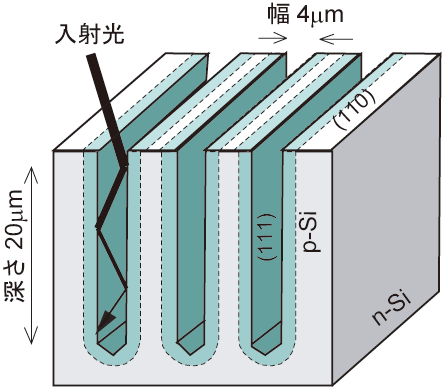 図1 垂直溝つきSi太陽電池 |
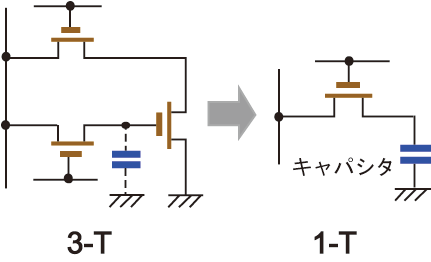 図2 DRAMセルの改良:3トランジスタセルから 1トランジスタ+1キャパシタヘ |
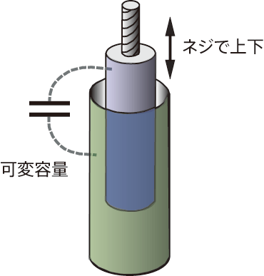 図3 同軸円筒のトリマーコンデンサー |
●太陽電池から着想したアイディア
そうこうしているうちにスタンフォード滞在中に参加した学会で印象的な発表を聴講した。その後いくら探しても発表論文が見つからず、情けないが学会名さえあやふやになってしまった。もしかしたら、ハードコピーが残らないゴードン・リサーチ・コンファレンスではないかと疑っている。 その発表はテキサスインスツルメンツ社のK.E.ビーン氏らが提案した太陽電池であり、図1に示すごとくSi(110)面にKOH水溶液で垂直な溝を多数造りつけた構造である。溝に入射した光は吸い込まれて消滅するために無効な反射光が極めて少なく、光電変換効率が上がるというものである。今でこそ、垂直の細い溝が形成できるドライエッチングがあるが、当時は等方性の溶液エッチングしかなく、ようやく開発が始まった円筒形プラズマエッチングもほぼ等方性であった。等方性エッチングでは半球状の穴しか得られない。したがって、アスペクト比が5のこの垂直なエッチング溝を見たときには鳥肌が立ったぐらいである。
同時期に図2に示すようにDRAMセルの構成が3トランジスタ型から1トランジスタ+1キャパシタ型に移行したという噂を聞いていた。光電子分光でSiの表面・界面を解析しようという研究者がなぜ畑違いのDRAMに興味を持ったか。ここで、無線機やオーディオアンプを造っていた“デバイス嗜好”がそうさせたのではないかと思う。無線機には共振周波数を精密に調整するためにトリマーコンデンサーという部品がある。これは図3に示すように円筒形のコンデンサーであり、内部の電極を入れ出しすることによって対向電極面積を変え、容量値を変化させる。この円筒形コンデンサーとSi垂直溝が頭の中で合体した。 トレンチキャパシタセル特許出願
集積回路は小さいほどコストが安い。一方、面積を増やしてキャパシタの値を大きければ信号も増大し安定な動作ができるだろうがコストも増大する。だったらSi基板に垂直な溝を形成してこの側壁をキャパシタの電極にすれば、面積を増やさずにキャパシタンスの値を増大できるから一石二鳥ではないかと考えた。すぐ当時の上司に「特許出願の明細書申請用紙を送ってくれ」と米国から手紙で頼んだ(まだインターネットはありません)。折り返し「今の研究に無関係な横道にそれず、留学先での研究をきちんと仕上げなさい」というものだった。この好奇心優先の横道嗜好は今も変わっていない。
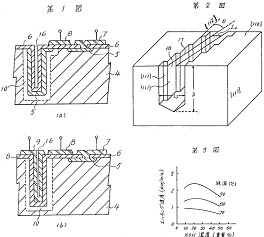 図4 最初のトレンチキャパシタDRAMセルの出願特許 (特願昭50-53883「半導体記憶装置」)の冒頭図面 |
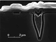 図5 最初に試作したトレンチキャパシタセル |
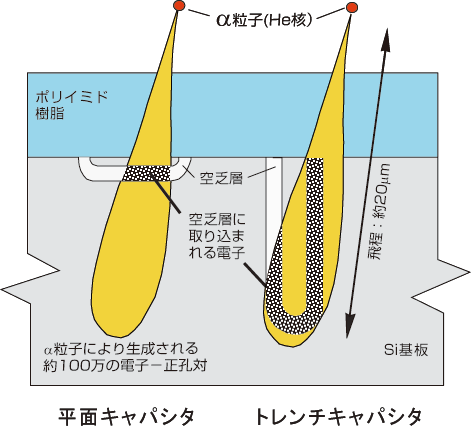 図6 α粒子の入射による電子−正孔対生成過程 |
この出願からたった1ヶ月後、日本のF社から、翌年には日本のT社、翌々年には日本のM社、N社、米国のT社、I社から同じ概念の特許が出願されている。ほんのタッチの差である。私がもう少し逡巡して出願が遅れていたら、今の私とは違った道を歩いていたに違いない。
本稿の主旨とはずれるので記載しないがこの発明とともにトレンチの応用と派生技術で様々なアイディアを出願した。二層ポリSi構造のDRAMや、今でこそ注目を浴びているSiの梁の側壁をチャネルとしたトランジスタ、さらには基板を貫通した垂直な溝を電極とするものなどである。一部のアイディアは製品化にもこぎつけ会社に貢献した。このトレンチキャパシタから派生した構造や技術は今の今でも研究対象にしている。早い話、私の“独創性”はほぼ30年前で飽和していたのである。 ここまではトレンチキャパシタの発案から特許出願までの経緯を述べた。次ぎに、製品開発経緯を述べ、何故、自社で製品化できなかったかを分析してみたい。ここには日本企業の開発の課題が縮図となって現れている。
1KビットDRAMが1970年に製品化されてから一世代3年毎に4倍に規模を拡大してきた。世代がすすむ毎にチップ面積を1.5倍に拡大、メモリセルをほぼ40%に縮小、そして回路の改良を加えて4倍化を実現してきた。セルの縮小は蓄積キャパシタ面積の縮小をもたらす。だが、安定な回路動作のためキャパシタ容量値を保たねばならないのでキャパシタ絶縁膜を薄くして補ってきた。その結果、電源電圧12Vでは絶縁破壊を引き起こすまでに薄くなった。これでは解が無い。当時日立では中央研究所の伊藤清男博士が発案した折り返しデータ線構成や5V単一電源ほか様々な挑戦的な技術で64Kビット開発に成功した。順調に製品化され、1K,4K、16Kと米国のメーカーが先導していた世界市場でとうとう日本の日立がトップメーカーとなった(その後4Mまでの4世代は日本のメーカーが先導してきた)。この“勝ち戦”はその後の研究開発に大きな影響を与えている。
トップを取った日立は様々な意味で余裕ができた。眠っていたトレンチキャパシタのアイディアの具現化を図ろうとの機運が高まり、1Mビットへの適用開発が始まった。完全結晶を理想とする技術者から「溝を掘り、結晶を傷つけるのは何事か」という批判があったのを懐かしく思い出す。試作は極めて順調で、当時まだ方向性が十分ではなかったドライエッチングによっても図5の様なセルができ、平面の2倍以上の容量値が実現できた。この結果を1982年の国際電子デバイス学会(IEDM)で発表した。この時代、日立は一目置かれていたためか多くのメーカーがトレースを開始した。
■1978年 スタックセル 小柳光正(日立中研)
■1982年 トレンチセル 角南英夫(日立中研)
■1984年 フラッシュメモリ 舛岡富士雄(東芝)
■1988年 トランジスタ移動度解析 高木真一(東芝)
■1989年 DELTAトランジスタ 久本大(日立中研)
■1990年 SiGe歪みトランジスタ 村上英一(日立中研)
受賞者に日立が多いのは、当時最先端の中央研究所で他社よりずっと多くのリソースを充て、かつ研究所としては多額の設備投資を続けた成果だと私は分析している。また、私を含め半分の3人が東北大学西澤潤一研究室出身であるのも偶然とはいえないような気がして興味深い。 製品化開発を覆った暗雲
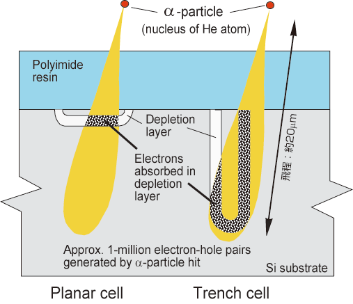
1Mビット製品化を目指したトレンチセルであったが試作評価段階で大きな障害が見つかった。それは当時DRAMの大規模化を止めるとまで騒がれたソフトエラーである。パッケージ樹脂などに含まれるトリウムやウランから発生するヘリウム核(α粒子)が固体と衝突すると最大約百万個の電子−正孔対を生成する。これはほぼ200fCの電荷量で、蓄積キャパシタに蓄える信号電荷量とほぼ同じである。ヒットした瞬間だけ一過性の記憶データ不良を誘発するのでソフトエラーと呼ばれる。トレンチキャパシタは図6に示すごとく基板に深く空乏層が伸びるので、まるでα線のセンサーのように効率よく電子を集めた。当時耐α線特性は最も耳目を集めていた話題であった。いくつかの改良構造も提案されたが次に述べる理由によってトレンチキャパシタの製品化は断念された。
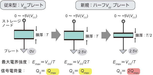 図7 ハーフVCCによる信号電荷量の増大 |
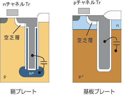 図8 ソフトエラー対策をしたセル構造 |
|
●1MビットDRAMは従来平面型に回帰
当時、DRAMの最大市場はIBMが率いている大型計算機で、高い信頼性を要求していた。IBMの採用は信頼性保証のお墨付きであり、多くのDRAMメーカーはこれを目指した。それでも採用されるのは最初に要求をクリヤした2,3社であり、半年の開発遅延は致命的となるという背景があった。その様な状況の下、三菱電機から従来のプレーナー(平面型)でも1Mビットが実現できる技術が発表された。これはハーフVCCと呼ばれるプレート電圧印加方式で、図7に示すように電源電圧の半分の2.5Vをプレートに印加することによって、キャパシタ絶縁膜の電界を半分にできる。この余裕を利用して絶縁膜の厚さを半減し、同じ面積で2倍の信号電荷量を実現する技術である。
このような背景の下、日立はトレンチキャパシタの製品化を見送り、プレーナーに回帰した。一方、IBM、シーメンス、東芝、TIなどは開発に成功し、1Mビットで製品化した。
● スタックキャパシタセルの台頭
実は日立内ではトレンチキャパシタセルに先んじてスタックキャパシタセルを研究していた。同じ職場で机を並べていた小柳光正博士(現東北大学教授)で、その成果を1978年のIEDMで発表した。前述のようにIEDM優秀発表に選ばれている。しかしまだ十分プレーナー型で製品が実現できる時代であったので社内の製品化は後回しになった。最初に製品化したのは、1Mビットでの富士通であった。スタックセルはほぼ従来技術で製品化できたので、業界の指向もスタックに傾き、日立は4M以後スタックセルを採用する。
いっぽう中央研究所のグループは図8に示すような抜本的な耐α線構造を提案したが、「熱さに懲りてなますを吹く」とは言い過ぎであろうか、以後トレンチセルの製品化が試みられることは無かった。現在のトレンチセル製品は図中右に基本構造を示す基板プレートを採用している。α粒子が生成する雑音電子を集める空乏層が極めて小さいのがわかろう。現在市場におけるスタック対トレンチの割合はおおよそ3:1である。前者はサムスン、エルピーダ、マイクロン、ハイニックス、後者は東芝、IBM、キモンダ(旧インフィニオン)などのメーカーがある。 空乏層の極小化によりソフトエラーに強い。
IEEE西澤潤一メダル受賞
本賞がアナウンスされたのは2002年である。マテリアルとデバイスの融合に対するめざましい功績に与えられるので、少し対象がちがうのかなという懸念はあったが、DRAM市場の二大セルを発明した西澤先生の弟子二人が、それらのアレー配置を発明した同僚との三人で申請するのは半ば義務であろうと思い、あえて申請に踏み切った。授賞式は2006年6月24日、ミネソタ州ミネアポリスでとりおこなわれた。その会場で、我々三名は1トランジスタセルの発明者、IBMのロバート・デナード博士に挨拶し感謝した。氏の発明が無ければ、少なくとも受賞の対象になった技術は生まれてこなかったのである。デナード博士はよく知られたスケーリング則の提唱者でもある。
IEEE表彰には、エジソン、グラハム・ベル、ロバート・ノイス、ジャック・キルビー、フォン・ノイマンなどの名を冠したメダルがあり、これらに並ぶジュンイチ・ニシザワ・メダルのステータス、栄誉は計り知れない。あらためて身の引き締まる思いである。
“独創”のトラウマ 西澤先生の教えを再び記すと「論文は読むな。他人と同じことはするな。独創を最優先せよ」――先生が自らこうおっしゃっていたかどうかは、40年余の時空を超えた今では実は定かでない。先生の背中から受けた印象が私にそう言わせているのである。先生はマスコミを通じ、生涯続けて限りなくメッセージを発信していらっしゃるので、間違ってはいないと勝手に思いこんでいる。 このトラウマは何か研究上で行動しようとするといつも頭をもたげる。その結果、先のわからない難題を選ぶことになる。「他人と違ったことをしたい」というのはどんな性格の発露なのだろう。今更変えようにも変えられない。まあ、分析は心理学者にまかせよう。 いっぽう、集積回路市場ではメモリもプロセッサも様々な障害に直面している。1GビットDRAMの製品化遅延、プロセッサの高速化終息宣言などですでにその兆候が現れている。
筆者は来年定年を迎えるが、これらの障害を乗り越える明確な解を見いだしていないのが心残りである。30年前に飽和してしまった“独創性”をもう一度奮い立たせるには何をすればよいかと考えてみたい。 最後に、トレンチDRAM開発を推進してくださった当時の部長の浅井彰二郎博士、集積回路設計のとりまとめをしていただいた伊藤清男博士、机を並べて互いに刺激し合った小柳光正博士、また中央研究所での試作を行っていただいた多くのエンジニヤに感謝してペンを置きます。
Receipt of IEEE Jun-ichi Nishizawa Medal
I was given 2006 IEEE Jun-ichi Nishizawa Medal from IEEE together with Dr. Mitsumasa Koyanagi, Professor of Tohoku University and Dr. Kiyoo Ito, Hitachi Fellow. This medal which was founded in 2002 will be given to people who accomplish outstanding works in areas of semiconductor materials and devices. I was the first Japanese recipient together with them. My achievements are trench capacitor DRAM cell which is enevitable to hjigh-density DRAM's same as stack capacitor cell. Achivements of Dr. Koyanagi and Dr. Ito are stack capacitor cell and folded bit-lne arrangement, respectively. These achivements were done while all three recipients were working at Central Research Laboratory, Hitachi, Ltd.
Besides this medal, I received IEEE Paul Rappaport Award, IEEE Cledo Brunetti Award, and Tokyo Governor's Distinguished Inventor Award, IEEE Fellow, IEICE Fellow, JSAP Fellow. I would like to describe its development process of invention, patent application, successful implementation.
While, I was invited to publish an article of development process of trench capacitor in June and October 2006issues of Senior Semiconductor Association brochure. The contens are sumamrized here as well as in my book of "Patent Guide for Engineers".
A trench capacitor cell (tench cell) is that a storage capacitor of dynamic-random-access memory, DRAM is formed inside a trench dug into silicon substrate. As a big storage capacitor can be provided without enlarging its planar area, the trench capacitor as well as stack capacitor is enevitable in DRAM products. The usage of the trench and the stack capacitors in 2005 is shown below.
 |
●Started at a crystal set
A root of my engineering career was a crystal radio set at primary schohol. Enameled copper wires were put around a boddin, then a part of enamel was stripped off making electric contact area. I was skillful at picture drawing and handicraft, however, radio sound did not come out. Reading a technical book, I found a description that there might be a failure in the crystal. Even though I could not understand exactly, I got a lot of knowledge such that the crystal was made of Rochelle salt, what is frequency, tuning, detection, etc.
I was gradually getting enthusiastic to this hobby in junior high and high schools. I made four-vacuum tube radio receiver at first thensuper heterodyne short-wave radio receiver at last. I frequently went to Akihabara, I was very much impressed with fantastic used tranceivers disposed from US army. Armature radio hobby was in the golden age those days. I made a transmitter using a transmitter vacuum tube of 807. As I was learning very hard to pass an entrance examination of some university I could not afford to get a call sign of amateur radio license. Also I did not like to pick up very small voice out of very big background noises of short wave radio. If I had got an amateur radio license, I would have been respected with a vintage call sign of JA1 something.
In my university life, I was getting interested in audio rather than amateur radio. Choosing a unusual power vacuum tube, I designed a power amplifier looking for an appropriate transformer with adequate impedance matching. I was proud of only one audio amplifier in the world. But, I misunderstood that vacuum tubes could be operated at maximum rating, then the tube was soon broken with over loading. Then, I chose transistors in spite of vacuum tubes as power element, I made up more than 10 amplifiers. But only one still remains at present.
●Trauma given from Professor Nishizawa
I chose semiconductor as undergraduate and graduate thesis at Tohoku University. I was insolent enough to think that thesis concerning circuits was not deserved and I picked up processing as the thesis. I thought that my future job should differ from my hobby. If I had chosen circuits, my research life would be completely different.
A lesson which Professor Nishizawa taught us with his back is still a trauma for me. That is "do not read journal papers, do not the same thing of others, originality first". I was taught face to face only every six months however, this lesson was very serious to me. But I have realized the value of this lesson 10 and 20 years later.
Thesis of Master course was an observation of silicon epitaxial layer surface. As I could not get satisfactory results on suggested target, I have chosen other target. Even though I was scolded with this side trip, the results were pulished in "Semiconductor Research" magazine on motre than10 pages. I was so impressed with this management that the results were acknowledged. Even though I have been teaching these eight years, I could not make students get this kind of experiences.
●Semiconductor process development as may first job
Then, I was employed at Central Research laboratory, Hitachi, Ltd. in 1969. As first microprocessor and first DRAM were introduced in 1970, the coincidence of timingwas very lucky to me. I was engaged in projects of multilevel metallization and charge-coupled device, CCD which were widely developed in semiconductor field. When I had a chance to study abroad, I have chosen interface analysis at Professor William Spicer's laboratory at Stanford University to analyze CCD operation. During one year from 1973, I have done a research on CsO2 surface with photoemission spectroscopy. But, I could use a spectrometer for one week every six months, I got nervous that I could not make experiments against my will even though I could observe US circumstances in detail.
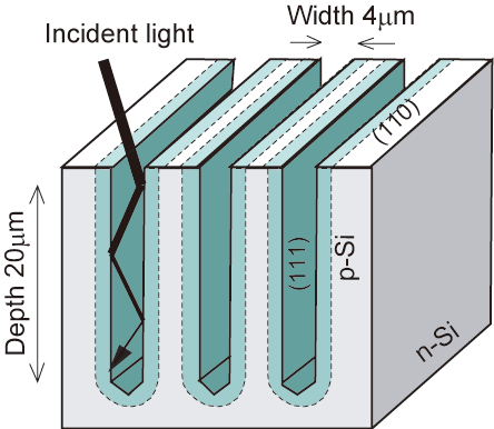 Fig. 1 A silicon solar cell with vertical trenches. |
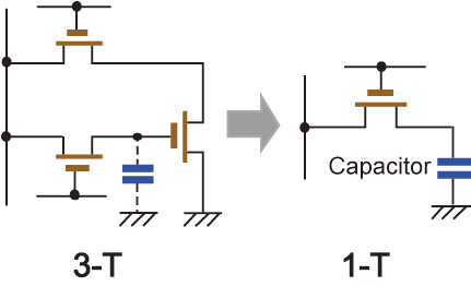 Fig. 2 Improvement of DRAM cell, from 3 transistors to 1 transistor and 1 capacitor. |
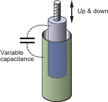 Fig. 3 A coaxial cylinder trimmer condenser. |
●Hint come from solar cell
While I was staying at Stanford University, I was so impressed with a publicaton presented at some conference. Afterwards, I was looking for the abstract, I failed in getting it. I am not sure at present what was the conference. I suspect that was Gordon Research Conference where no hard copies existed. That publication described a solar cell with steep trenches dug into silicon (110)-oriented substrate with preferential KOH etchant, as shown in Fig. 1. Incident lights are absorbed on the trench walls with multi-reflection on the wall surface resulting high conversion efficiency.
The anisotropic etching method to produce narrow steep trenches is well known today but there existed no anosotropic method but isotropic one. Even a barrel-type plasma etching method which was gegun to be developed was isotropic. With the isotropic etching, we can get only hemi-spherical holes. Therefore, when I took a look at that steep trenches of which aspect ratio exceeded 5, I felt I had goose bumps.
At the same period, I have heard from a report that DRAM cell configuration moved from 3 transistors to 1 transistor and 1 capacitor. Why an engineer who was analyzing CsO2 surface with photoemission spectroscopy got interested in this topic in different field? I think that a device-oriented attitude cultivated at his hobbies of hand-made audio and amateur radio turned his head to the topic.
Radio receiver contain trimmer condensers which trim resonant frequency. This is a cylindrical one, as shown in Fig. 3, of which up-and-down inner electrode can vary capacitance value. This cylindrical condenser and silicon trench get together in my brain.
Patent application Smaller integrated circuit chip generates less cost. While, bigger capacitance with enlarged capacitance area provides more stable operation, but the cost is increased. Then, I got an idea that the same capacitance area with trench capacitor provided larger capacitance. Soon I sent a letter to my boss to ask him to send a patent application format. Internet did not exist at that time. He sent me a letter saying "do not enter a byway, concentrate yourself on present research target." My preference to byway does not change to date.
| > |
|
 |
|
|
Fig. 4 Principal nfigures of the first patent application of the trench cell,
(Tokugansho-50-53883 "Semiconductor memory ndevice") |
Fig. 5 The very first trench cell fabricated. | Fig. 6 Electron-hole pairs generated with alpha-particle hit. |
After I returned back to Japan in September 1974, I could not abandone the idea, then I applied a patent on May 7, 1975. That was Tokugansho 50-53883 entitled "semiconductor memory device". I put a lot of application examples into the patent leading to powerful tool for obtaining the patent right. Principal drawings of the patent atatement are shown Fig. 4. As the concept of this patent application was not understood, this was not applied to overseas. I should have done a tough negociation.
One month after this application, a patent with the same concept was applied from Japanese F-company. Next year, from japanese T-company, the second next year, from Japanese M- and N-comanies, and American T- and I-companies. I won the patent by a touch. If I had applied the patent several month later, I would have walked on a different way from the present one.
I have applied a lot of derivative ideas but I do not describe them here because subjects of them differ from that of this article. They were (1) double-polysilicon gate DRAM, (2) MOS devices with sidewall channels, and (3) through-silicon via (TSV) electrode which are now popular in semiconductor products. SOme part of ideas have been implemented in products. Now I am trying to realize these ideas which I conceived. To be honest, my originality was dried up almost 30 years ago.
Invention and patent application of the trench cell are described above, then, the development procedure will be explained hereafter. In addition, I would like to analyze how the trench cell was not abandoned in productization. There may exist a miniature of Japanese development scheme.
DRAM has been increasing its volume by four times every generation of 3 years since first 1-Kbit DRAM product was introduced to the market in 1970. As the generation goes, 4-fold increase in its volume has been achieved while its chip size has been increased by 1.5 times with reduced memory cell size of 40% in addition to cuircuit innoivations. The reduction of the cell size also causes the decrease in storage capacitor area. As the storage capacitance vbalue should be kept to be almost constant to provide stable circuit operation, capacitor insulator has been decreased in thickness.
As the result of the thickness decrease, electric field strength across the storage insulator has become close to capastrophic breakdown of the insulator at 12-V power supply voltage. There was no solution in this scaling sheme. While, Hitachi has succeeded in a trial development of 64-Kbit DRAM TEG(test element group) with innovative 5-V single power supply and a folded-bit line arrangement which was proposed by Dr. K. Itoh. Subsequent to the US makers who hahave led 1-K, 4-K, and 16-K DRAM markets, Hitachi has won a leader's position at 64 Kbit. Then up to 4 Mbit, Japanese makers have continued to possesses leader's position. The winning has a great influence on subsequent research and development.
Hitachi who won the 64-Kbit generation could afford to challenge to the development of 1-Mbit DRAM with trench capacitor. There arose a criticism such that it was no good to dig trenches into perfect silicon crystal. We succeeded in a trial fabrication resulting in more than twice capacitance with a trench as shown in Fi. 5 even with unmatured plasma etchig. This result was presented at International ElecrtronDevices Meeting (IEDM) in 1982. As Hitachi was a leader at that era, a lot of makeres have begun to trace our trial.
* stack cell by M. Koyanagi (Hitachi) in 1978,
* trench cell by H. Sunami (Hitachi) in 1982,
* flash memory by F. Masuoka (Toshiba) in 1984,
* mobilitycharacterization by S. Takagi (Toshiba),
* DELTA transistor by D. Hisamoto (Hitachi) in 1989, and
* SiGe strain transistor by E. Murakami (Hitachi) in 1990.
I guess one of reasons that Hitachi won many might be that a lot of resouces with plenty of investiment were devoting to silicon interated circuit development at Central Research Labotaroty as a corporate laboraotry. In addition, it is interesting three recipients out of six have studied at Prof. J. Nishizawa Laboratory at Tohoku University.
The trench cell was being aimed at applying to 1-Mbit DRAM product, we have found a big difficulty. That was soft-error which was estimated to stop further integration DRAM. Trace elements of U and Th atoms which are contained in package resin make a particles (He nuclei) causing generation of about one million pairs of electrons and holes. The amount of charges is almost 200 fC which is almost equal to charges stored in a storage capacitor. Since an error occurs only at a moment when a particle hits memory array, this phenomenon is called "soft error".
As a depletion layer of a trench cell is stretching deeply into silicon substrate, the trench cell was efficiently acting as an a particle sensor. Soft error problem was recognaized to be the most serious problem. Even though several improved structures were proposed, productization of the trench cell was abandoned as is described below.
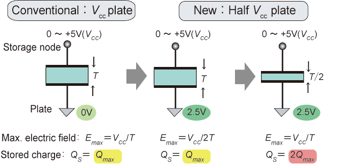 Fig.7 Increased charges with HalfVCC plate configuration. |
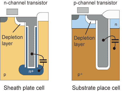 Fig. 8 Soft-error hardened cells. |
||
●Return back to conventional planar cell at 1-Mbit DRAM
Mainframe conputers whic have been led by IBM required very high realiabilityfor memories. As adoption of the memory by IBM namely meant the guarantee of high reliability, a lot of DRAM makers aimed to be one of suppliers. However, only two or three makers could be an supplier. Thus, only half-year delay of product shipment might lose their business in high-reliability DRAM market.
Under such circumstances, Mitsubishi proposed a technology which enabled to make 1-Mbit with a conventional planar cell. This was named "half Vcc plate" which provided 2.5-V voltage application to the plate, as shown in Fig. 7, resulting in one half that of electric field across the insulator. Thus, it provided twice as much stored charges with one half thickness of capacitor insulator.
Utilizing this half Vcc plate scheme, Hitachi returned back to the coventional planar cell. While, IBM, Siemens, Toshiba, TI succeeded in productization of the trech cell at 1-Mbit DRAM era.
● Stack capacitor cell gained power
Hitachi has in reality been developing a stack capacitor cell (stach cell) prior to the trench cell. Its developer was Dr. Koyanagi (professor at Tohokuj University at present) ,who was working close to my desk, presented the successful results 1t 1978 IEDM. This presentation was also selected as one of 58 outstanding presentatons of IEDM as shown above. As planar cell still offered sufficient performance at taht time, productization of the stack cell was postponed. First winner of stack cell product was Fujitsu at 1-Mbit era. As the stack cell was able to be manufactured with conventional fabrication technologies, most of DRAM makers began to adopt the stack cell. From 4-Mbit DRAM, Hitachi has been manufacturing the stach cell.
Even though the developing group at Hitachi Central Research Laboratory proposed trench cell structures with improved soft error imunity as shown in Fig. 8, no trench cell was tried to be developed since then. Present trench cell in products has been adopting the substrate plate cell as shown in Fig. 8. The depletion layer which gathers charges generated with a particle hit is very small. A ratio of stack to trench is about 3 at present in 2006 in commodity DRAM market. Samsung, Hynix, Micron, Elpida, etc. have been emplying the stack, otherwise, Toshiba, IBM, Qimonda (former Infineon), and some Taiwan manufacturers, the trench.
Jun-ichi Nishizawa medal was establised in 2002. As this medal is given to person(s) who has achieved an outstanding contribution to merging of materials and devices, I was afraid that I might not deserve this medal. However, I dared to apply thinking that two students who have learned at Nishizawa Laboratory with a colleage who invented folded bit-line arrangement had a duty to apply the medal.
The ceremony was held in Mineapolis on June 24, 2006. At that party, we met Dr. Dennard and expressed our sincere thanks to hi. He was a very famous guy who invented one-transistor DRAM cell. Without his invention, we would not have received this medal. He is also well-known proposer of scaling thory.
Among IEEE medals, there are those of Thomas Edison, Graham Bell, Robert Noyce, Jack Kilby, and Von Neumann. The glory of the status of Jun-ichi Nishizawa Medal is enormous.
PI have got a trauma of "origibnality" which I was given from Prof. Nioshizawa. That was "do not read other journal papers, do not do the same things which others are doing, originality first". As fourty years have passed, I did not remember whether professor really told himself . I make myself to say that looking at his back. Professor has been continually telling that through mass media, therefore I think it is surely true.
When I begin to do something at R&D, I always feel this trauma. Thsu I happen to meet some difficulty. What kind of character is this? It may be a subject of psychologist. I do not mind. Meanwhile, meories and processors are facing various difficulties in integrated circuit market. Some delay of 1-Gbit DRAM shipment and saturation of operating frequency of micro processors should be that sign.I will retire next year but I regret slightly that I do not find solutions to them. I would like to regenerate "originality" again, which was satujrated 30 years ago.
I would like to express sincere thanks to Dr. S. Asai for his promoting trench cell development, Dr. K. Itoh for his supervising of circuit innovation, Dr. M. Koyanagi for his working hard together, and all other engineers for their trial fabrications of trench cell.