 |
■研究開発経歴 / R&D History ・ 経歴 / History ・野鳥撮影 / Bird Photograph |
|
■登録特許 / Registered patents ■日本出願 /Japanese pat. applied ■海外出願 / International patents ■トピックス / Topics ・ 特許の勧め / Invitation to patent ・ 特許分割 / Patent dividing ・ クロスライセンス/Cross license |
|
[主要更新 ] '16-11-14: 本サイト再構築 '05-6:原www.suna.cc開設 |
|
| 通番 |
出願番号 |
公開番号 |
国際公開 番号 |
登録番号 |
発明の名称 |
出願人(略称) |
発明者 |
| 262 | 2003-117826 | 2004-327568 | 半導体装置 | 科学技術振興機構 | 吉川 公麿;岩田 穆;角南 英夫;マタウシユ ハンスユルゲン;横山 新;芝原 健太郎;中島 安理;小出 哲士;エ−ビ−エム ハルン ウル ラシツド;渡辺 慎治 | ||
| 261 | 平10-532326 | WO98/ 028789 | 半導体記憶装置及びその製造方法 | 日立製作所 | 山中 俊明;木村 紳一郎;松岡 秀行;角南 英夫;伊藤 清男;関口 知紀;阪田 健;宮崎 祐行 | ||
| 260 | 平09-274090 | 平11-111929 | 3554666 | 半導体メモリ装置 | 日立製作所; ヒタチ ヨ−ロツパ |
角南 英夫;伊藤 清男;島田 寿一;中里 和郎;水田 博 | |
| 259 | 平09-240030 | 平11- 87541 | 3489973 | 柱状構造を有する半導体装置 | 日立製作所 | 中里 和郎;水田 博;島田 寿一;角南 英夫;伊藤 清男;手島 達也;峰 利之 | |
| 258 | 平08-333372 | 平10-173148 | 半導体記憶装置 | 日立製作所 | 松岡 秀行;山中 俊明;角南 英夫;木村 紳一郎;伊藤 清男 | ||
| 257 | 平08-176305 | 平09-198865 | 半導体メモリ、半導体集積回路装置、制御回路、論理回路、および論理回路の特性を調節する方法 | 日立製作所;テキサスインストルメンツ | 秋葉 武定;大鳥 浩;橘川 五郎;中村 正行;角南 英夫;エイデイン イ− ヒスロツプ | ||
| 256 | 平08-124331 | 平08-274281 | 2679702 | 半導体記憶装置の製造方法 | 日立製作所 | 木村 紳一郎;川本 佳史;加賀 徹;角南 英夫 | |
| 255 | 平03- 28257 | 平05-308132 | 2069680 | 半導体メモリの製造方法 | 日立製作所 | 角南 英夫;久礼 得男;川本 佳史 | |
| 254 | 平03- 25993 | 平03-268357 | 2099446 | 半導体装置の製造方法 | 日立製作所 | 角南 英夫;久礼 得男;川本 佳史;田村 誠男;宮尾 正信 | |
| 253 | 平02-295338 | 平03-174768 | 1899602 | 半導体メモリ | 日立製作所 | 角南 英夫;久礼 得男;川本 佳史;宮尾 正信 | |
| 252 | 平02-126709 | 平03- 16124 | 半導体装置 | 日立製作所 | 角南 英夫;久礼 得男;川本 佳史 | ||
| 251 | 平01-152215 | 平03- 20550 | 2747024 | 清浄室 | 日立製作所; 日立プラント; 日立建設設計 |
斉木 篤;角南 英夫;矢木 邦博;川本 佳史;船越 清彦;亀山 正義;倉水 勝;高森 昶光;河合 秀直;鈴木 道夫 | |
| 250 | 平01- 27417 | 平02-?? 354 | 1745808 | 大規模半導体メモリ | 日立製作所 | 角南 英夫;久礼 得男;川本 佳史 | |
| 249 | 平01-? 6004 | 平02-? 3179 | 1694776 | メモリ装置 | 日立製作所 | 湊 修;増原 利明;下東 勝博;増田 弘生;神垣 良昭;萩原 吉宗;角南 英夫;酒井 芳男;武田 英次 | |
| 248 | 平01-? 6003 | 平02-? 3178 | 1694775 | メモリ装置 | 日立製作所 | 湊 修;増原 利明;下東 勝博;増田 弘生;神垣 良昭;萩原 吉宗;角南 英夫;酒井 芳男;武田 英次 | |
| 247 | 昭63-250914 | 平02- 98970 | 2021944 | 縦型接合型電界効果トランジスタの製造方法 | 産業技術総合研究所 | 中川 清和;宮尾 正信;山口 憲;角南 英夫 | |
| 246 | 昭63-150281 | 平01-152661 | 1862143 | 半導体メモリ | 日立製作所 | 角南 英夫;久礼 得男;川本 佳史;宮尾 正信 | |
| 245 | 昭63- 69426 | 平01- 53433 | 3009146 | 半導体集積回路 | 日立製作所 | 角南 英夫;西野 寿一;三沢 豊;加藤 隆彦 | |
| 244 | 昭62-314024 | 平01-155656 | 半導体記憶装置 | 日立製作所 | 木村 紳一郎;川本 佳史;角南 英夫 | ||
| 243 | 昭62-310821 | 平01-152660 | 2606857 | 半導体記憶装置の製造方法 | 日立製作所 | 加賀 徹;川本 佳史;角南 英夫 | |
| 242 | 昭62-275784 | 平01-120050 | 半導体記憶装置 | 日立製作所; 日立超L |
木須 輝明;妹尾 幸治;久礼 得男;角南 英夫;木村 紳一郎 | ||
| 241 | 昭62-253631 | 平01- 96949 | 半導体装置 | 日立製作所 | 木村 紳一郎;川本 佳史;角南 英夫 | ||
| 240 | 昭62-247819 | 平01- 91009 | 薄膜の平坦性評価装置 | 日立製作所 | 高橋 繁;角南 英夫;船越 清彦;奥平 定之;田村 誠男;吉広 尚次;恒川 助芳;加賀 徹 | ||
| 239 | 昭62-223922 | 平01- 67982 | 無摺動スイツチ | 日立製作所 | 角南 英夫;西野 寿一;宮内 克己 | ||
| 238 | 昭62-190024 | 平01- 35963 | 不揮発性メモリ | 日立製作所 | 神力 博;西岡 泰城;角南 英夫;向 喜一郎;山本 英明 | ||
| 237 | 昭62-187539 | 平01- 32629 | エツチング装置 | 日立製作所 | 角南 英夫;奥平 定之;川本 佳史;久礼 得男;田村 誠男;吉広 尚次;恒川 助芳;船越 清彦;加賀 徹;高橋 繁 | ||
| 236 | 昭62-185481 | 平01- 30248 | 溝上絶縁膜の形成方法 | 日立製作所 | 加賀 徹;木村 紳一郎;久礼 得男;川本 佳史;角南 英夫 | ||
| 235 | 昭62-166782 | 平01- 11360 | 半導体記憶装置 | 日立製作所; 日立超L |
大木 長斗司;牧野 藤八;加賀 徹;角南 英夫;清水 昭博 | ||
| 234 | 昭62-153306 | 昭63-318130 | 2634595 | 半導体製造装置 | 日立製作所 | 加賀 徹;角南 英夫;田村 誠男;奥平 定之;船越 清彦;吉広 尚次;恒川 助芳;高橋 繁 | |
| 233 | 昭62-148961 | 昭63-313823 | プラズマ処理方法及び装置 | 日立製作所 | 恒川 助芳;角南 英夫;奥平 定之;田村 誠男;船越 清彦;吉広 尚次;加賀 徹;高橋 繁 | ||
| 232 | 昭62-139728 | 昭63-304259 | レイアウト方法 | 日立製作所 | 松沢 敏晴;角南 英夫;茂庭 明美;加賀 徹;木村 紳一郎 | ||
| 231 | 昭62-139716 | 昭63-304124 | 温度感知器 | 日立製作所 | 角南 英夫 | ||
| 230 | 昭62-128297 | 昭63-293967 | 2569048 | 半導体メモリの製造方法 | 日立製作所; 日立超L |
木須 輝明;高浜 高;木村 紳一郎;角南 英夫;大賀 一弘 | |
| 229 | 昭62-128124 | 昭63-293814 | ウエハ処理の情報伝達方法 | 日立製作所 | 奥平 定之;角南 英夫;船越 清彦;田村 誠男;吉広 尚次;恒川 助芳;高橋 繁;加賀 徹 | ||
| 228 | 昭62-121233 | 昭63-288009 | ウエハとウエハ処理工程管理方法 | 日立製作所 | 角南 英夫;田村 誠男;奥平 定之;船越 清彦;吉広 尚次;加賀 徹;高橋 繁;恒川 助芳 | ||
| 227 | 昭62-114633 | 昭63-281466 | 自己整合接続法 | 日立製作所 | 角南 英夫;須藤 敬己 | ||
| 226 | 昭62-114620 | 昭63-280293 | 2559405 | 透光性平面スピ−カ付き平面表示装置 | 日立製作所 | 御子柴 茂生;福島 正和;鴻上 明彦;武田 康嗣;塚田 俊久;角南 英夫 | |
| 225 | 昭62- 99763 | 昭62-271450 | 半導体装置の製造方法 | 日立製作所 | 角南 英夫;川本 佳史 | ||
| 224 | 昭62- 97394 | 昭63-263757 | 半導体記憶装置およびその製造方法 | 日立製作所; 日立超L |
木須 輝明;木村 紳一郎;角南 英夫;大木 長斗司 | ||
| 223 | 昭62- 97300 | 昭63-263758 | 半導体メモリ | 日立製作所 | 角南 英夫;木村 紳一郎;加賀 徹 | ||
| 222 | 昭62- 77416 | 昭63-245954 | 半導体メモリ | 日立製作所 | 角南 英夫;木村 紳一郎;加賀 徹 | ||
| 221 | 昭62- 63761 | 昭63-232318 | 微細パタ−ン形成方法 | 日立製作所 | 松沢 敏晴;角南 英夫;茂庭 明美 | ||
| 220 | 昭62- 24529 | 昭63-193555 | 2602219 | 半導体記憶装置 | 日立製作所 | 木村 紳一郎;川本 佳史;加賀 徹;角南 英夫 | |
| 219 | 昭62- 24528 | 昭63-193556 | 半導体メモリ | 日立製作所 | 角南 英夫;加賀 徹;木村 紳一郎 | ||
| 218 | 昭62- 18329 | 昭63-187664 | 半導体装置 | 日立製作所; 日立超L |
清水 昭博;角南 英夫 | ||
| 217 | 昭61-281722 | 昭63-136559 | 2674992 | 半導体記憶装置におけるプレ−ト配線形成法 | 日立製作所 | 加賀 徹;木村 紳一郎;角南 英夫 | |
| 216 | 昭61-281716 | 昭63-136558 | 半導体記憶装置とその製造方法 | 日立製作所 | 加賀 徹;木村 紳一郎;角南 英夫 | ||
| 215 | 昭61-179920 | 昭63- 37613 | 半導体装置の製造方法 | 日立製作所 | 角南 英夫;茂庭 昌弘;蕨迫 光紀;宮尾 正信 | ||
| 214 | 昭61-142992 | 昭63-? 1052 | 半導体記憶装置とその製造方法 | 日立製作所 | 木村 紳一郎;角南 英夫;久礼 得男 | ||
| 213 | 昭61-104651 | 昭61-263153 | 1690710 | 半導体記憶装置およびその製造方法 | 日立製作所 | 角南 英夫;西松 茂 | |
| 212 | 昭61- 60645 | 昭62-219659 | MOS型半導体記憶装置 | 日立製作所 | 木村 紳一郎;西岡 泰城;神力 博;佐久間 憲之;角南 英夫 | ||
| 211 | 昭61- 15617 | 昭62-175036 | 信号伝送路 | 日立製作所 | 茂庭 昌弘;花谷 昌一;角南 英夫 | ||
| 210 | 昭61-?? 546 | 昭61-165965 | 高集積化電源素子 | 日立製作所 | 角南 英夫;宮内 克己;兼堀 恵一;工藤 徹一 | ||
| 209 | 昭60-279263 | 昭62-139318 | 低温気相成長法 | 日立製作所 | 高橋 亮吉;井上 洋典;角南 英夫 | ||
| 208 | 昭60-269397 | 昭62-130550 | MIS型キヤパシタの製造方法 | 日立製作所 | 木村 紳一郎;西岡 泰城;神力 博;佐久間 憲之;角南 英夫 | ||
| 207 | 昭60-267533 | 昭62-128168 | 2127461 | 半導体メモリの製造方法 | 日立製作所 | 木村 紳一郎;角南 英夫 | |
| 206 | 昭60-235144 | 昭62- 95873 | 電界効果トランジスタ | 日立製作所 | 山本 秀一;村上 英一;木村 紳一郎;大倉 理;蕨迫 光紀;角南 英夫 | ||
| 205 | 昭60-235137 | 昭62- 95859 | 半導体装置の製造方法 | 日立製作所 | 大倉 理;楠川 喜久雄;角南 英夫 | ||
| 204 | 昭60-175817 | 昭62- 36807 | 単結晶薄膜の製造方法 | 日立製作所 | 楠川 喜久雄;大倉 理;角南 英夫 | ||
| 203 | 昭60-167561 | 昭62- 29161 | 半導体装置 | 日立製作所 | 平岩 篤;小沢 正実;矢木 邦博;角南 英夫;久礼 得男 | ||
| 202 | 昭60-167559 | 昭62- 29160 | 半導体装置の製造方法 | 日立製作所 | 平岩 篤;矢木 邦博;角南 英夫;久礼 得男 | ||
| 201 | 昭60-148392 | 昭62-? 9664 | 半導体装置 | 日立製作所 | 大倉 理;楠川 喜久雄;角南 英夫 | ||
| 200 | 昭60-134095 | 昭61-292914 | 半導体装置の製造方法 | 日立製作所 | 平岩 篤;矢木 邦博;角南 英夫;久礼 得男 | ||
| 199 | 昭60-126032 | 昭61-284911 | 単結晶薄膜の形成方法 | 日立製作所 | 楠川 喜久雄;大倉 理;角南 英夫 | ||
| 198 | 昭60-114076 | 昭61-272923 | 拡散法 | 日立製作所 | 角南 英夫;久礼 得男;平岩 篤;和田 恭雄 | ||
| 197 | 昭60-110475 | 昭61-269307 | 1978272 | CVD装置 | 日立製作所 | 高橋 亮吉;角南 英夫;井上 洋典;鈴木 誉也 | |
| 196 | 昭60- 95901 | 昭61-255056 | 2008503 | 半導体メモリ | 日立製作所 | 角南 英夫;久礼 得男;平岩 篤;和田 恭雄 | |
| 195 | 昭60- 93745 | 昭61-252656 | 1973686 | 半導体装置およびその製造方法 | 日立製作所 | 茂庭 昌弘;蕨迫 光紀;角南 英夫 | |
| 194 | 昭60- 93604 | 昭61- 10255 | 1485472 | 半導体装置の製造方法 | 日立製作所 | 増原 利明;角南 英夫;神垣 良昭;橋本 哲一 | |
| 193 | 昭60- 44797 | 昭61-204960 | マイクロキヤパシタ形成方法 | 日立製作所 | 角南 英夫;久礼 得男;平岩 篤;和田 恭雄 | ||
| 192 | 昭60- 42636 | 昭62-194572 | シミユレ−シヨン方法 | 日立製作所 | 高橋 亮吉;松田 正敏;井坂 光明;角南 英夫 | ||
| 191 | 昭60- 32625 | 昭61-193422 | 単結晶層の形成方法 | 日立製作所 | 角南 英夫;茂庭 昌弘;蕨迫 光紀;宮尾 正信 | ||
| 190 | 昭60- 30371 | 昭61-190976 | 半導体装置 | 日立製作所 | 山口 憲;堀内 勝忠;西村 玲子;角南 英夫 | ||
| 189 | 昭60- 26230 | 昭61-187355 | 半導体キヤパシタ | 日立製作所 | 角南 英夫 | ||
| 188 | 昭60- 23085 | 昭61-183969 | 電界効果トランジスタ | 日立製作所 | 角南 英夫 | ||
| 187 | 昭60-? 5762 | 昭61- 50368 | 半導体装置の製造方法 | 日立製作所; 日本電信電話 |
神垣 良昭;伊藤 清男;堀 陵一;川本 佳史;角南 英夫;橋本 哲一;村本 進 | ||
| 186 | 昭59-272920 | 昭61-151449 | 電子線回折装置 | 日立製作所 | 茂庭 昌弘;宮尾 正信;蕨迫 光紀;角南 英夫;斉藤 栄 | ||
| 185 | 昭59-257581 | 昭60-157261 | 半導体装置の製造方法 | 日立製作所 | 角南 英夫 | ||
| 184 | 昭59-211376 | 昭61- 91434 | 1876136 | クリ−ンル−ム | 日立製作所; 日立プラント |
斉木 篤;鈴木 道夫;角南 英夫;浅井 彰二郎;牧 道義;浅見 欽一郎 | |
| 183 | 昭59-211375 | 昭61- 91433 | クリ−ンル−ム | 日立製作所; 日立プラント |
斉木 篤;鈴木 道夫;角南 英夫;浅井 彰二郎;牧 道義;浅見 欽一郎 | ||
| 182 | 昭59-178318 | 昭61- 58234 | 現像シユミレ−シヨン方法 | 日立製作所 | 松沢 敏晴;梅谷 征雄;角南 英夫 | ||
| 181 | 昭59-137140 | 昭61- 17293 | 半導体メモリ装置 | 日立製作所 | 木村 勝高;堀 陵一;伊藤 清男;角南 英夫 | ||
| 180 | 昭59-133150 | 昭61- 13634 | プラズマ処理装置 | 日立製作所 | 村上 英一;木村 紳一郎;蕨迫 光紀;三宅 潔;角南 英夫 | ||
| 179 | 昭59-133148 | 昭61- 13626 | プラズマ処理装置 | 日立製作所 | 木村 紳一郎;村上 英一;蕨迫 光紀;三宅 潔;角南 英夫 | ||
| 178 | 昭59-121726 | 昭60- 35567 | 半導体メモリ | 日立製作所 | 酒井 芳男;小柳 光正;角南 英夫;橋本 哲一 | ||
| 177 | 昭59-121725 | 昭60- 35566 | 半導体装置の製造方法 | 日立製作所 | 酒井 芳男;小柳 光正;角南 英夫;橋本 哲一 | ||
| 176 | 昭59-101684 | 昭60-246619 | 1994525 | 半導体装置の製造方法 | 日立製作所 | 茂庭 昌弘;宮尾 正信;角南 英夫 | |
| 175 | 昭59- 81750 | 昭60-226185 | 1968465 | 縦型電界効果トランジスタ | 日立製作所 | 蕨迫 光紀;角南 英夫 | |
| 174 | 昭59- 45468 | 昭60-189962 | 半導体集積回路 | 日立製作所 | 角南 英夫 | ||
| 173 | 昭59- 45467 | 昭60-189964 | 半導体メモリ | 日立製作所 | 谷田 雄二;角南 英夫;湊 修;青木 正和;高木 克明;堀口 真志;田村 誠男 | ||
| 172 | 昭59- 21698 | 昭60-167474 | マイクロチヤネルトランジスタ | 日立製作所 | 角南 英夫;宿利 章二;田村 誠男 | ||
| 171 | 昭59- 16106 | 昭59-139193 | 1636023 | メモリ装置 | 日立製作所 | 湊 修;増原 利明;下東 勝博;増田 弘生;神垣 良昭;萩原 吉宗;角南 英夫;酒井 芳男;武田 英次 | |
| 170 | 昭59- 11966 | 昭60-158664 | 半導体装置およびその製造方法 | 日立製作所 | 小林 伸好;岩田 誠一;山本 直樹;角南 英夫 | ||
| 169 | 昭59- 11919 | 昭60-158616 | 半導体装置の製造方法 | 日立製作所 | 大倉 理;角南 英夫;楠川 喜久雄 | ||
| 168 | 昭59- 11906 | 昭60-158667 | 半導体装置 | 日立製作所 | 茂庭 昌弘;宮尾 正信;角南 英夫 | ||
| 167 | 昭58-246948 | 昭60-140861 | マイクロキヤパシタ半導体メモリ | 日立製作所 | 角南 英夫;大倉 理;宮尾 正信;楠川 喜久雄;茂庭 昌弘;木村 紳一郎;蕨迫 光紀;久礼 得男 | ||
| 166 | 昭58-246947 | 昭60-140860 | 半導体装置 | 日立製作所 | 井倉 康雄;西村 玲子;山口 憲;萩原 隆旦;角南 英夫 | ||
| 165 | 昭58-246928 | 昭60-140812 | 半導体装置の製造方法 | 日立製作所 | 大倉 理;角南 英夫;楠川 喜久雄 | ||
| 164 | 昭58-243836 | 昭60-136318 | 半導体装置の製造方法 | 日立製作所 | 木村 紳一郎;村上 英一;蕨迫 光紀;角南 英夫;三宅 潔 | ||
| 163 | 昭58-242022 | 昭60-134468 | 半導体装置 | 日立製作所 | 角南 英夫;宿利 章二;田村 誠男 | ||
| 162 | 昭58-236167 | 昭60-128622 | エツチング法 | 日立製作所 | 角南 英夫;田村 誠男 | ||
| 161 | 昭58-236160 | 昭60-128654 | 1833142 | 半導体集積回路 | 日立製作所 | 角南 英夫;大倉 理;木村 紳一郎 | |
| 160 | 昭58-222036 | 昭60-115254 | 半導体装置とその製造方法 | 日立製作所 | 久礼 得男;川本 佳史;角南 英夫;矢木 邦博 | ||
| 159 | 昭58-217719 | 昭59-103374 | 1501554 | 半導体記憶装置 | 日立製作所 | 角南 英夫;西松 茂 | |
| 158 | 昭58-217718 | 昭59-103373 | 1542864 | 半導体記憶装置 | 日立製作所 | 角南 英夫;西松 茂 | |
| 157 | 昭58-217717 | 昭59-103372 | 半導体記憶装置 | 日立製作所 | 角南 英夫;西松 茂 | ||
| 156 | 昭58-217716 | 昭59-103371 | 1542863 | 半導体記憶装置 | 日立製作所 | 角南 英夫;西松 茂 | |
| 155 | 昭58-207426 | 昭60-100425 | 集積回路電極の形成方法 | 日立製作所 | 角南 英夫 | ||
| 154 | 昭58-207425 | 昭60-100464 | 半導体装置 | 日立製作所 | 角南 英夫 | ||
| 153 | 昭58-194269 | 昭60- 86815 | 半導体装置の製造方法 | 日立製作所 | 茂庭 昌弘;楠川 喜久雄;大倉 理;宮尾 正信;角南 英夫 | ||
| 152 | 昭58-186748 | 昭60- 79770 | 半導体メモリ | 日立製作所 | 久礼 得男;角南 英夫 | ||
| 151 | 昭58-180252 | 昭60- 74555 | 半導体装置 | 日立製作所 | 角南 英夫;久礼 得男 | ||
| 150 | 昭58-177957 | 昭60- 70757 | 1816391 | 半導体集積回路 | 日立製作所 | 角南 英夫 | |
| 149 | 昭58-177952 | 昭60- 70758 | 2069347 | 半導体メモリ | 日立製作所 | 角南 英夫;大倉 理;宮尾 正信;楠川 喜久雄;茂庭 昌弘;木村 紳一郎;蕨迫 光紀;久礼 得男 | |
| 148 | 昭58-172933 | 昭60- 65561 | 半導体メモリ | 日立製作所 | 角南 英夫;伊藤 清男;本間 紀之 | ||
| 147 | 昭58-172931 | 昭60- 65559 | 半導体メモリ | 日立製作所 | 角南 英夫;久礼 得男;大倉 理 | ||
| 146 | 昭58-156244 | 昭59- 56764 | 半導体メモリ | 日立製作所 | 角南 英夫;川本 佳史 | ||
| 145 | 昭58-146448 | 昭60- 38863 | 半導体装置の製造方法 | 日立製作所 | 川本 佳史;角南 英夫;堀 陵一;和田 恭雄;水谷 巽 | ||
| 144 | 昭58-146394 | 昭60- 38855 | 1741435 | 半導体装置およびその製造方法 | 日立製作所 | 久礼 得男;角南 英夫;川本 佳史 | |
| 143 | 昭58-146388 | 昭60- 38809 | 半導体装置の製造方法 | 日立製作所 | 楠川 喜久雄;大倉 理;角南 英夫;宮尾 正信;茂庭 昌弘 | ||
| 142 | 昭58-141036 | 昭60- 32355 | 半導体装置とその製造方法 | 日立製作所 | 久礼 得男;角南 英夫;川本 佳史 | ||
| 141 | 昭58-127688 | 昭60- 21553 | 1854762 | 三次元集積回路 | 日立製作所 | 角南 英夫;大倉 理;楠川 喜久雄;宮尾 正信;茂庭 昌弘 | |
| 140 | 昭58-115840 | 昭60-? 9154 | 半導体メモリとその製造方法 | 日立製作所 | 茂庭 昌弘;宮尾 正信;大倉 理;楠川 喜久雄;酒井 芳男;角南 英夫 | ||
| 139 | 昭58-115831 | 昭60-? 9166 | 半導体装置の製造方法 | 日立製作所 | 角南 英夫;岩田 誠一;山本 直樹;小林 伸好 | ||
| 138 | 昭58-102600 | 昭59-228762 | マルチゲ−トトランジスタ | 日立製作所 | 角南 英夫 | ||
| 137 | 昭58- 95727 | 昭59-222959 | 1926047 | 半導体メモリ | 日立製作所 | 角南 英夫;大倉 理;楠川 喜久雄;宮尾 正信;蕨迫 光紀 | |
| 136 | 昭58- 90687 | 昭59-217323 | 単結晶シリコンの製造方法 | 日立製作所 | 宮尾 正信;大倉 理;楠川 喜久雄;茂庭 昌弘;角南 英夫 | ||
| 135 | 昭58- 84182 | 昭59-210653 | 半導体装置の製造方法 | 日立製作所 | 和田 恭雄;佐藤 朗;久米 均;川本 佳史;伊藤 清男;堀 陵一;角南 英夫 | ||
| 134 | 昭58- 59243 | 昭59-186346 | 電極接続法 | 日立製作所 | 角南 英夫;岩田 誠一;山本 直樹;小林 伸好 | ||
| 133 | 昭58- 55066 | 昭59-182566 | 半導体装置 | 日立製作所 | 井坂 光明;酒井 芳男;角南 英夫 | ||
| 132 | 昭58- 37391 | 昭59-163816 | 単結晶シリコン膜の製造方法 | 日立製作所 | 宮尾 正信;大倉 理;楠川 喜久雄;茂庭 昌弘;三宅 潔;蕨迫 光紀;角南 英夫 | ||
| 131 | 昭58- 35812 | 昭59-161860 | 半導体メモリ装置 | 日立製作所 | 木村 勝高;堀 陵一;伊藤 清男;角南 英夫 | ||
| 130 | 昭58- 30719 | 昭59-158514 | 半導体装置の製造方法 | 日立製作所 | 大倉 理;宮尾 正信;楠川 喜久雄;蕨迫 光紀;角南 英夫 | ||
| 129 | 昭58- 22741 | 昭59-149047 | 半導体装置 | 日立製作所 | 西岡 泰城;本間 紀之;向 喜一郎;角南 英夫;木村 紳一郎 | ||
| 128 | 昭57-215424 | 昭59-106146 | 半導体メモリ | 日立製作所 | 鳥谷部 達;角南 英夫;浅井 彰二郎 | ||
| 127 | 昭57-193413 | 昭59- 84416 | 単結晶薄膜の製造方法 | 日立製作所 | 楠川 喜久雄;大倉 理;宮尾 正信;蕨迫 光紀;角南 英夫 | ||
| 126 | 昭57-193412 | 昭59- 84488 | 半導体装置 | 日立製作所 | 茂庭 昌弘;宮尾 正信;大倉 理;蕨迫 光紀;角南 英夫;鳥谷部 達;山口 憲;萩原 隆旦 | ||
| 125 | 昭57-192478 | 昭59- 82761 | 1677755 | 半導体メモリ | 日立製作所 | 角南 英夫;久礼 得男;川本 佳史;宮尾 正信 | |
| 124 | 昭57-187436 | 昭59- 78534 | ドライエツチング装置 | 日立製作所 | 角南 英夫;飯島 普平;橋本 哲一 | ||
| 123 | 昭57-147535 | 昭59- 39070 | 半導体装置およびその製造方法 | 日立製作所; 日立マイコン |
大賀 一弘;和田 恭雄;角南 英夫 | ||
| 122 | 昭57- 87945 | 昭58-206160 | 半導体装置の製造方法 | 日立製作所 | 和田 恭雄;角南 英夫;矢木 邦博;奥平 定之;久礼 得男;川本 佳史;松田 正敏 | ||
| 121 | 昭57- 84763 | 昭58-202550 | 1861603 | 半導体装置の製造方法 | 日立製作所 | 角南 英夫;久礼 得男;川本 佳史 | |
| 120 | 昭57- 84762 | 昭58-202560 | 半導体装置およびその製造方法 | 日立製作所 | 久礼 得男;角南 英夫;川本 佳史 | ||
| 119 | 昭57- 83013 | 昭58-200541 | エツチング方法 | 日立製作所 | 久礼 得男;角南 英夫;池田 清治;川本 佳史 | ||
| 118 | 昭57- 81427 | 昭58-199553 | 半導体装置の製造方法 | 日立製作所 | 久礼 得男;角南 英夫;和田 恭雄;奥平 定之 | ||
| 117 | 昭57- 79960 | 昭58-197824 | 半導体装置 | 日立製作所 | 恒川 助芳;本間 喜夫;小松 英雄;林田 哲哉;佐藤 朗;角南 英夫 | ||
| 116 | 昭57- 36418 | 昭58-154256 | 1714010 | 半導体装置 | 日立製作所 | 角南 英夫;久礼 得男;川本 佳史;田村 誠男;宮尾 正信 | |
| 115 | 昭57- 18740 | 昭58-137245 | 1714004 | 大規模半導体メモリ | 日立製作所 | 角南 英夫;久礼 得男;川本 佳史 | |
| 114 | 昭57-? 7592 | 昭58-125295 | 集積化電源素子 | 日立製作所 | 角南 英夫;下東 勝博;宮内 克己;兼堀 恵一;工藤 徹一 | ||
| 113 | 昭56-164185 | 昭58- 66328 | 半導体装置の製造方法 | 日立製作所 | 宮尾 正信;武田 英次;大倉 理;久米 均;角南 英夫;田村 誠男;夏秋 信義;吉広 尚次;徳山 巍 | ||
| 112 | 昭56-160193 | 昭58- 61622 | 単結晶薄膜の製造方法 | 日立製作所 | 田村 誠男;吉広 尚次;夏秋 信義;宮尾 正信;大倉 理;角南 英夫;徳山 巍 | ||
| 111 | 昭56-131521 | 昭58- 33870 | 半導体装置 | 日立製作所 | 角南 英夫;増田 弘生;神垣 良昭;下東 勝博;武田 英次 | ||
| 110 | 昭55-113512 | 昭57- 37852 | 1211177 | 半導体集積回路およびその回路プログラム方法 | 日立製作所 | 湊 修;増原 利明;酒井 芳男;下東 勝博;増田 弘生;角南 英夫;神垣 良昭;武田 英次;萩原 吉宗 | |
| 109 | 昭54-134165 | 昭56- 58244 | 1213702 | 半導体集積回路およびその回路プログラム方法 | 日立製作所 | 湊 修;増原 利明;角南 英夫;酒井 芳男;武田 英次;下東 勝博;増田 弘生;神垣 良昭;萩原 吉宗 | |
| 108 | 昭54-125404 | 昭56- 50531 | 1211158 | 半導体集積回路とその回路プログラム方法 | 日立製作所 | 増原 利明;湊 修;下東 勝博;増田 弘生;角南 英夫;酒井 芳男;神垣 良昭;武田 英次;萩原 吉宗 | |
| 107 | 昭54-115293 | 昭56- 40270 | 1475350 | 半導体メモリの製造方法 | 日立製作所 | 角南 英夫;川本 佳史 | |
| 106 | 昭54-114183 | 昭56- 38866 | 1465967 | 半導体装置の製造方法 | 日立製作所 | 角南 英夫;川本 佳史 | |
| 105 | 昭54- 97301 | 昭56- 23771 | 半導体メモリ | 日立製作所 | 酒井 芳男;小柳 光正;角南 英夫;橋本 哲一 | ||
| 104 | 昭53-114627 | 昭55- 41738 | 1259532 | 半導体装置の製造方法 | 日立製作; 日本電信電話 |
角南 英夫;宮崎 隆雄 | |
| 103 | 昭53-103945 | 昭55- 30845 | 1524265 | 不揮発性記憶装置の製造方法 | 日立製作所 | 谷田 雄二;萩原 隆旦;角南 英夫;伊藤 容吉;近藤 隆二;南 真一 | |
| 102 | 昭53- 18469 | 昭54-111783 | 半導体装置の製造方法 | 日立製作所 | 角南 英夫;川本 佳史 | ||
| 101 | 昭52- 82931 | 昭54- 18684 | 1300205 | 半導体装置の製造方法 | 日立製作所; 日本電信電話 |
神垣 良昭;伊藤 清男;角南 英夫;川本 佳史;谷田 雄二;小柳 光正;水尾 祥一;橋本 哲一;村本 進 | |
| 100 | 昭52- 82930 | 昭54- 18683 | 1399344 | 半導体装置の製造方法 | 日立製作所; 日本電信電話 |
神垣 良昭;伊藤 清男;堀 陵一;川本 佳史;角南 英夫;橋本 哲一;村本 進 | |
| 99 | 昭52- 67901 | 昭54-? 3470 | エツチング法 | 日立製作所 | 谷田 雄二;角南 英夫 | ||
| 98 | 昭52- 65760 | 昭54-?? 990 | 1394501 | MOS型集積回路の製造方法 | 日立製作所 | 増田 弘生;角南 英夫;伊藤 清男 | |
| 97 | 昭52- 63381 | 昭53-149774 | 1193170 | 集積回路製造法 | 日立製作所; 日本電信電話 |
角南 英夫;西松 茂;村本 進 | |
| 96 | 昭52- 59772 | 昭53-145572 | 半導体装置の製造方法 | 日立製作所 | 和田 恭雄;薄井 洪夫;角南 英夫 | ||
| 95 | 昭52- 22688 | 昭53-108385 | 半導体装置の製造方法 | 日立製作所 | 神山 孝光;角南 英夫 | ||
| 94 | 昭52- 22686 | 昭53-108384 | 半導体装置の製造方法 | 日立製作所 | 角南 英夫;小柳 光正;西松 茂 | ||
| 93 | 昭52- 22684 | 昭53-108383 | 半導体装置とその製造方法 | 日立製作所 | 堀 陵一;伊藤 清男;久保 征治;角南 英夫;橋本 哲一;西松 茂 | ||
| 92 | 昭52- 22683 | 昭53-108382 | 1328415 | 半導体装置 | 日立製作所 | 角南 英夫;湊 修;増原 利明;酒井 芳男;和田 恭雄 | |
| 91 | 昭52- 22679 | 昭53-108381 | 半導体装置の製造方法 | 日立製作所 | 角南 英夫;飯島 晋平 | ||
| 90 | 昭52- 22674 | 昭53-108378 | 半導体装置の製造方法 | 日立製作所 | 小柳 光正;角南 英夫;西松 茂;橋本 哲一 | ||
| 89 | 昭52- 19242 | 昭53-105369 | 不純物濃度検出法 | 日立製作所 | 角南 英夫;和田 恭雄 | ||
| 88 | 昭52-? 4926 | 昭53- 90887 | 半導体メモリ装置の製造方法 | 日立製作所 | 増田 弘生;角南 英夫 | ||
| 87 | 昭52-? 4921 | 昭53- 90869 | 半導体装置の製造方法 | 日立製作所 | 飯島 晋平;角南 英夫 | ||
| 86 | 昭52-? 2889 | 昭53- 89381 | 集積回路の製造方法 | 日立製作所 | 角南 英夫 | ||
| 85 | 昭52-? 2888 | 昭53- 89328 | 半導体メモリ | 日立製作所 | 角南 英夫 | ||
| 84 | 昭52-? 2395 | 昭53- 94780 | 半導体装置の製造方法 | 日立製作所 | 和田 恭雄;角南 英夫;西松 茂 | ||
| 83 | 昭52-??? 32 | 昭53- 85166 | 半導体装置の製造方法 | 日立製作所 | 谷田 雄二;角南 英夫;和田 恭雄 | ||
| 82 | 昭51-134053 | 昭53- 59372 | マスク合せ方法 | 日立製作所 | 松沢 敏晴;角南 英夫;柳沢 寛;橋本 哲一 | ||
| 81 | 昭51-134051 | 昭53- 59371 | マスク合わせ装置 | 日立製作所 | 松沢 敏晴;角南 英夫 | ||
| 80 | 昭51-123810 | 昭53- 49969 | 半導体記憶装置 | 日立製作所 | 小柳 光正;角南 英夫 | ||
| 79 | 昭51-122776 | 昭53- 48483 | 半導体装置の製造方法 | 日立製作所 | 小柳 光正;角南 英夫 | ||
| 78 | 昭51-122775 | 昭53- 48482 | 半導体装置の製造方法 | 日立製作所 | 角南 英夫;小柳 光正 | ||
| 77 | 昭51-114722 | 昭53- 40287 | 半導体装置の製造方法 | 日立製作所 | 甲藤 久郎;角南 英夫 | ||
| 76 | 昭51-114719 | 昭53- 40291 | 1364079 | 半導体装置の製造方法 | 日立製作所 | 増原 利明;角南 英夫;神垣 良昭;橋本 哲一 | |
| 75 | 昭51-107794 | 昭53- 33586 | 半導体装置の製造方法 | 日立製作所 | 角南 英夫;西松 茂;武田 英次 | ||
| 74 | 昭51-101656 | 昭53- 27372 | 半導体装置の製造方法 | 日立製作所 | 角南 英夫;神垣 良昭;橋本 哲一 | ||
| 73 | 昭51- 85086 | 昭53- 10985 | 半導体メモリの製造方法 | 日立製作所 | 角南 英夫 | ||
| 72 | 昭51- 81982 | 昭53- 10337 | 1041928 | エツチング法 | 日立製作所 | 角南 英夫;西松 茂 | |
| 71 | 昭51- 77818 | 昭53-? 4475 | エツチング方法 | 日立製作所 | 角南 英夫;和田 恭雄;長谷川 昇雄 | ||
| 70 | 昭51- 76385 | 昭53-? 3077 | 電荷移送装置 | 日立製作所 | 角南 英夫;小柳 光正;増原 利明;小池 紀雄 | ||
| 69 | 昭51- 76384 | 昭53-? 3081 | 集積回路配線法 | 日立製作所 | 角南 英夫;小柳 光正;増原 利明;小池 紀雄 | ||
| 68 | 昭51- 75562 | 昭53-? 1428 | 半導体メモリ | 日立製作所 | 小柳 光正;角南 英夫;佐藤 喜久治 | ||
| 67 | 昭51- 75554 | 昭53-? 1481 | 集積回路の配線法 | 日立製作所 | 角南 英夫;小柳 光正 | ||
| 66 | 昭51- 74351 | 昭53-?? 979 | 半導体装置の製造方法 | 日立製作所 | 湊 修;久保 征治;角南 英夫 | ||
| 65 | 昭51- 66532 | 昭52-149989 | 半導体メモリ | 日立製作所 | 角南 英夫;小柳 光正 | ||
| 64 | 昭51- 63614 | 昭52-147017 | 1216311 | 固体撮像素子 | 日立製作所 | 小池 紀雄;増原 利明;角南 英夫;小柳 光正 | |
| 63 | 昭51- 61153 | 昭52-144979 | トランジスタ | 日立製作所 | 角南 英夫;和田 恭雄 | ||
| 62 | 昭51- 60014 | 昭52-143770 | マスク合せ方法 | 日立製作所 | 角南 英夫 | ||
| 61 | 昭51- 57809 | 昭52-141590 | 半導体メモリセル | 日立製作所 | 増原 利明;角南 英夫;小池 紀雄;小柳 光正 | ||
| 60 | 昭51- 53281 | 昭52-137275 | 半導体素子分離法 | 日立製作所 | 角南 英夫 | ||
| 59 | 昭51- 49952 | 昭52-133755 | 集積回路製造法 | 日立製作所 | 角南 英夫 | ||
| 58 | 昭51- 46585 | 昭52-130287 | 集積回路製造法 | 日立製作所 | 角南 英夫;谷田 雄二;西松 茂;橋本 哲一 | ||
| 57 | 昭51- 23316 | 昭52-107857 | 膜厚測定法 | 日立製作所 | 本田 征夫;角南 英夫;橋本 哲一 | ||
| 56 | 昭51- 21142 | 昭52-104879 | 半導体装置の製造方法 | 日立製作所 | 神垣 良昭;角南 英夫 | ||
| 55 | 昭51- 16041 | 昭52- 99777 | マスク合せ方法 | 日立製作所 | 角南 英夫 | ||
| 54 | 昭51-? 2809 | 昭52- 86783 | 半導体装置の製造方法 | 日立製作所 | 長谷川 昇雄;角南 英夫;柳沢 寛;堂田 喜久雄;山本 直樹 | ||
| 53 | 昭51-? 2808 | 昭52- 86779 | 半導体装置 | 日立製作所 | 角南 英夫;小柳 光正 | ||
| 52 | 昭51-? 2070 | 昭52- 86085 | 半導体装置の製造方法 | 日立製作所 | 角南 英夫 | ||
| 51 | 昭50-153325 | 昭52- 77592 | 半導体装置の製造方法 | 日立製作所 | 角南 英夫 | ||
| 50 | 昭50-125316 | 昭52- 49767 | 半導体装置 | 日立製作所 | 角南 英夫 | ||
| 49 | 昭50-111622 | 昭52- 35983 | 電界効果トランジスタの製造方法 | 日立製作所 | 角南 英夫 | ||
| 48 | 昭50-104009 | 昭52- 28868 | 半導体装置 | 日立製作所 | 角南 英夫;山本 直樹 | ||
| 47 | 昭50- 98585 | 昭52- 23274 | 自己整合型半導体装置 | 日立製作所 | 角南 英夫;川本 佳史;長谷川 昇雄 | ||
| 46 | 昭50- 96712 | 昭52- 20982 | 表面加工・表面処理の制御方法 | 日立製作所 | 川本 佳史;角南 英夫 | ||
| 45 | 昭50- 89251 | 昭52- 13781 | 接合型電界効果トランジスタ | 日立製作所 | 角南 英夫 | ||
| 44 | 昭50- 89250 | 昭52- 13777 | 集積回路製造法 | 日立製作所 | 角南 英夫 | ||
| 43 | 昭50- 76633 | 昭52-? 2175 | エツチング法 | 日立製作所 | 角南 英夫 | ||
| 42 | 昭50- 70832 | 昭51-147271 | 半導体記憶装置 | 日立製作所 | 角南 英夫;小柳 光正;堀 陵一;西松 茂 | ||
| 41 | 昭50- 70830 | 昭52-? 2174 | 1096508 | 自己整合エツチング法 | 日立製作所 | 角南 英夫 | |
| 40 | 昭50- 70829 | 昭51-147269 | 1344386 | 電界効果トランジスタ | 日立製作所 | 角南 英夫 | |
| 39 | 昭50- 58599 | 昭51-134584 | 掃引可変容量 | 日立製作所 | 角南 英夫;西松 茂 | ||
| 38 | 昭50- 58598 | 昭51-134586 | 集積回路配線法 | 日立製作所 | 角南 英夫 | ||
| 37 | 昭50- 53883 | 昭51-130178 | 1264351 | 半導体記憶装置 | 日立製作所 | 角南 英夫;西松 茂 | |
| 36 | 昭50- 41335 | 昭51-117033 | 写真蝕刻法 | 日立製作所 | 角南 英夫;和田 恭雄;柳沢 寛 | ||
| 35 | 昭50- 35565 | 昭51-111071 | 半導体装置 | 日立製作所 | 角南 英夫;川本 佳史;西松 茂 | ||
| 34 | 昭50- 17920 | 昭51- 93638 | 不揮発性記憶装置の制御装置 | 日立製作所 | 近藤 隆二;角南 英夫;堀内 勝忠 | ||
| 33 | 昭50-? 6259 | 昭51- 81578 | 半導体装置 | 日立製作所 | 角南 英夫;西松 茂;芦川 幹雄 | ||
| 32 | 昭49-17616 | 昭50-114181 | 電荷移送装置 | 日立製作所 | 角南 英夫 | ||
| 31 | 昭48-108394 | 昭50-61193 | 半導体光検出装置 | 日立製作所 | 小池 紀雄;角南 英夫;芦川 幹雄 | ||
| 30 | 昭48-101200 | 昭50-54376 | 湿度検出装置 | 日立製作所 | 角南 英夫 | ||
| 29 | 昭48- 71715 | 昭50- 22584 | 1319716 | 電荷移送装置 | 日立製作所 | 角南 英夫 | |
| 28 | 昭48- 69792 | 昭50- 20625 | 電荷移送装置 | 日立製作所 | 角南 英夫 | ||
| 27 | 昭48- 57945 | 昭50- 10042 | 不揮発性半導体記憶装置 | 日立製作所 | 神垣 良昭;堀内 勝忠;角南 英夫;伊藤 容吉 | ||
| 26 | 昭48- 57944 | 昭50- 10041 | 不揮発メモリ読み出し半導体装置 | 日立製作所 | 角南 英夫 | ||
| 25 | 昭48- 57942 | 昭50- 10039 | 不揮発性半導体記憶装置 | 日立製作所 | 角南 英夫;堀内 勝忠;伊藤 容吉 | ||
| 24 | 昭48- 55621 | 昭50- 12981 | デイジタルアナログ変換不揮発性半導体記憶装置 | 日立製作所 | 角南 英夫;堀内 勝忠 | ||
| 23 | 昭48- 38708 | 昭49-127581 | 991381 | 電荷移送装置 | 日立製作所 | 角南 英夫 | |
| 22 | 昭48- 29036 | 昭49-118378 | 無間隙電極電荷移送装置 | 日立製作所 | 角南 英夫 | ||
| 21 | 昭48-? 9516 | 昭49- 98972 | 高速電荷移送装置 | 日立製作所 | 角南 英夫;久保 征治;竹本 一八男 | ||
| 20 | 昭47-111140 | 昭49- 69090 | ドリフト電荷移送装置 | 日立製作所 | 角南 英夫 | ||
| 19 | 昭47- 88664 | 昭49- 48253 | 電荷移送装置 | 日立製作所 | 角南 英夫;神垣 良昭 | ||
| 18 | 昭47- 62411 | 昭49- 23555 | アナログメモリ | 日立製作所 | 角南 英夫;大矢 雄一郎;神垣 良昭;伊藤 容吉 | ||
| 17 | 昭47- 55057 | 昭49- 70578 | 927026 | 電荷移送形アナログデイジタル変換半導体装置 | 日立製作所 | 角南 英夫;神垣 良昭;伊藤 容吉 | |
| 16 | 昭47- 34362 | 昭48-102980 | 表面電位検出素子 | 日立製作所 | 角南 英夫;神垣 良昭 | ||
| 15 | 昭47- 25636 | 昭48- 94372 | 全面被覆電荷移送素子 | 日立製作所 | 角南 英夫;神垣 良昭;伊藤 谷吉 | ||
| 14 | 昭47-? 6972 | 昭48- 77726 | 電荷移送形パタ−ン認識装置 | 日立製作所 | 角南 英夫;神垣 良昭;伊藤 容吉 | ||
| 13 | 昭47-? 5202 | 昭48- 75176 | 電荷移送半導体装置 | 日立製作所 | 増田 弘生;増原 利明;久保 征治;角南 英夫 | ||
| 12 | 昭47-? 1656 | 昭48- 74179 | 1007028 | 自己バイアス形電荷移送素子 | 日立製作所 | 伊藤 容吉;角南 英夫;神垣 良昭 | |
| 11 | 昭46- 97119 | 昭48- 61015 | 867810 | 電荷移送撮像装置 | 日立製作所 | 角南 英夫;神垣 良昭 | |
| 10 | 昭46- 97118 | 昭48- 61014 | 電荷移送素子における画像処理方法 | 日立製作 | 角南 英夫;神垣 良昭;高岡 スミ子;伊藤 容吉 | ||
| 9 | 昭46- 97117 | 昭48- 61081 | 移送方向可換電荷移送素子 | 日立製作所 | 角南 英夫;伊藤 容吉;神垣 良昭;高岡 スミ子 | ||
| 8 | 昭46- 91510 | 昭48- 56380 | 積分型電荷移送素子 | 日立製作所 | 角南 英夫;伊藤 容吉;神垣 良昭 | ||
| 7 | 昭46- 89938 | 昭48- 55674 | 907678 | 電荷移送素子における信号伝達方法及び装置 | 日立製作所 | 神垣 良昭;角南 英夫;伊藤 容吉 | |
| 6 | 昭46- 89023 | 昭48- 54878 | 919809 | アナログ電荷移送素子 | 日立製作所 | 角南 英夫;神垣 良昭;伊藤 容吉 | |
| 5 | 昭46- 81693 | 昭48- 47234 | 高速電荷移送素子 | 日立製作所 | 角南 英夫;神垣 良昭;伊藤 容吉 | ||
| 4 | 昭46- 81691 | 昭48- 47233 | 859898 | 電荷移送形素子を用いたX−Y双方向シフトアレ− | 日立製作所 | 角南 英夫;伊藤 容吉;猪瀬 文之;神垣 良昭 | |
| 3 | 昭46- 75456 | 昭48- 42684 | 電荷移送形素子 | 日立製作所 | 神垣 良昭;角南 英夫;伊藤 容吉 | ||
| 2 | 昭46- 70397 | 昭48- 40385 | 電荷移送形素子 | 日立製作所 | 角南 英夫;神垣 良昭 | ||
| 1 | 昭46- 38676 | 昭48-? 6680 | 920616 | 電荷移送形素子 | 日立製作所 | 伊藤 容吉;角南 英夫 | |
| Publication Number | Title | Publication Date | Publication Country | Assignee/Applicant Name | Inventor Name | |
1 |
US3814955 | CHARGE COUPLED SEMICONDUCTOR ELEMENT WITH NOISE CANCELLATION | 1974/6/4 | US | Hitachi, Ltd. | Itoh; Yokichi|Sunami; Hideo |
2 |
US3852801 | CHARGE-COUPLED SEMICONDUCTOR DEVICE PROVIDED WITH BIASING CHARGES | 1974/12/3 | US | Hitachi, Ltd. | Itoh; Yokichi|Sunami; Hideo|Kamigaki; Yoshiaki |
3 |
US4013897 | Information signal transfer method and a charge transfer | 1977/3/22 | US | Hitachi, Ltd. | Kamigaki; Yoshiaki|Sunami; Hideo|Itoh; Yokichi |
4 |
US4041521 | Shift array for pattern information processing device utilizing charge coupled semiconductor device | 1977/8/9 | US | Hitachi, Ltd. | Sunami; Hideo|Itoh; Yokichi|Inose; Fumiyuki|Kamigaki; Yoshiaki |
5 |
US4177391 | Charge transfer semiconductor device | 1979/12/4 | US | Hitachi, Ltd. | Sunami; Hideo|Kubo; Masaharu|Takemoto; Iwao |
6 |
US4210993 | Method for fabricating a field effect transistor | 1980/7/8 | US | Hitachi, Ltd. | Sunami; Hideo |
7 |
US4355374 | Semiconductor memory device | 1982/10/19 | US | Hitachi, Ltd. | Sakai; Yoshio|Koyanagi; Mitsumasa|Sunami; Hideo|Hashimoto; Norikazu |
8 |
US4358093 | Steel strip continuous annealing furnace | 1982/11/9 | US | Kawasaki Steel Corporation | Shimoyama; Yuji|Yanagishima; Fumiya|Sunami; Hideo|Suzuki; Munetoshi|Yamamoto; Hiromasa|Sakamoto; Gunji |
9 |
US4363471 | Steel strip continuous annealing apparatus | 1982/12/14 | US | Kawasaki Steel Corporation | Yanagishima; Fumiya|Shimoyama; Yuji|Sunami; Hideo|Ida; Yukio|Katsushima; Goji|Suzuki; Munetoshi|Ohnishi; Takeo |
10 |
US4363472 | Steel strip continuous annealing apparatus | 1982/12/14 | US | Kawasaki Steel Corporation | Shimoyama; Yuji|Yanagishima; Fumiya|Sunami; Hideo|Ida; Yukio|Katsushima; Goji|Ohnishi; Takeo|Fukushima; Takeo |
11 |
US4455495 | Programmable semiconductor integrated circuitry including a programming semiconductor element | 1984/6/19 | US | Hitachi, Ltd. | Masuhara; Toshiaki|Minato; Osamu|Shimohigashi; Katsuhiro|Masuda; Hiroo|Sunami; Hideo|Sakai; Yoshio|Kamigaki; Yoshiaki|Takeda; Eiji|Hagiwara; Yoshimune |
12 |
US4498951 | Method of manufacturing single-crystal film | 1985/2/12 | US | Hitachi, Ltd. | Tamura; Masao|Yoshihiro; Naotsugu|Natsuaki; Nobuyoshi|Miyao; Masanobu|Ohkura; Makoto|Sunami; Hideo|Tokuyama; Takashi |
13 |
US4561909 | Method of manufacturing T-3 grade low temper black plates | 1985/12/31 | US | Kawasaki Steel Corporation | Sunami; Hideo|Kuguminato; Hideo|Izumiyama; Yoshio|Yanagishima; Fumiya|Obara; Takashi|Mochizuki; Kazuo |
14 |
US4641279 | Semiconductor memory device having a dummy cell and a memory cell which is twice the size of the dummy cell | 1987/2/3 | US | Hitachi, Ltd. | Kimura; Katsutaka|Hori; Ryoichi|Ito; Kiyoo|Sunami; Hideo |
15 |
US4656492 | Insulated gate field effect transistor | 1987/4/7 | US | Hitachi, Ltd. | Sunami; Hideo|Masuda; Hiroo|Kamigaki; Yoshiaki|Shimohigashi; Katsuhiro|Takeda; Eiji |
16 |
US4670768 | Complementary MOS integrated circuits having vertical channel FETs | 1987/6/2 | US | Hitachi, Ltd. | Sunami; Hideo|Ohkura; Makoto|Kimura; Shinichiro |
17 |
US4683838 | Plasma treatment system | 1987/8/4 | US | Hitachi, Ltd. | Kimura; Shin-Ichiro|Murakami; Eiichi|Warabisako; Terunori|Miyake; Kiyoshi|Sunami; Hideo |
18 |
US4692994 | Process for manufacturing semiconductor devices containing microbridges | 1987/9/15 | US | Hitachi, Ltd. | Moniwa; Masahiro|Warabisako; Terunori|Sunami; Hideo |
19 |
US4693173 | Clean room | 1987/9/15 | US | Hitachi Plant Engineering & Construction Co., Ltd.|Hitachi, Ltd. | Saiki; Atsushi|Suzuki; Michio|Sunami; Hideo|Asai; Shojiro|Maki; Michiyoshi|Asami; Kinichiro |
20 |
US4742018 | Process for producing memory cell having stacked capacitor | 1988/5/3 | US | Hitachi, Ltd. | Kimura; Shinichiro|Sunami; Hideo |
21 |
US4751557 | Dram with FET stacked over capacitor | 1988/6/14 | US | Hitachi, Ltd. | Sunami; Hideo|Kure; Tokuo|Kawamoto; Yoshifumi|Tamura; Masao|Miyao; Masanobu |
22 |
US4860071 | Semiconductor memory using trench capacitor | 1989/8/22 | US | Hitachi, Ltd. | Sunami; Hideo|Kure; Tokuo|Hiraiwa; Atsushi|Wada; Yasuo |
23 |
US4873203 | Method for formation of insulation film on silicon buried in trench | 1989/10/10 | US | Hitachi, Ltd. | Kaga; Toru|Kimura; Shinichiro|Kure; Tokuo|Kawamoto; Yoshifumi|Sunami; Hideo |
24 |
US4873560 | Dynamic random access memory having buried word lines | 1989/10/10 | US | Hitachi, Ltd. | Sunami; Hideo|Kimura; Shinichiro|Kaga; Toru |
25 |
US4901128 | Semiconductor memory | 1990/2/13 | US | Hitachi, Ltd. | Sunami; Hideo|Kure; Tokuo|Miyao; Masanobu|Kawamoto; Yoshifumi|Shimohigashi; Katsuhiro|Sakai; Yoshio|Minato; Osamu|Masuhara; Toshiaki|Koyanagi; Mitsumasa|Shimizu; Shinji |
26 |
US4918502 | Semiconductor memory having trench capacitor formed with sheath electrode | 1990/4/17 | US | Hitachi, Ltd. | Kaga; Toru|Kimura; Shinichiro|Sunami; Hideo |
27 |
US4937641 | Semiconductor memory and method of producing the same | 1990/6/26 | US | Hitachi, Ltd. | Sunami; Hideo|Ohkura; Makoto|Miyao; Masanobu|Kusukawa; Kikuo|Moniwa; Masahiro|Kimura; ShinIchiro|Warabisako; Terunori|Kure; Tokuo |
28 |
US4967247 | Vertical dynamic random access memory | 1990/10/30 | US | Hitachi, Ltd | Kaga; Toru|Kawamoto; Yoshifumi|Sunami; Hideo |
29 |
US4984030 | Vertical MOSFET DRAM | 1991/1/8 | US | Hitachi, Ltd. | Sunami; Hideo|Kure; Tokuo|Kawamoto; Yoshifumi|Tamura; Masao|Miyao; Masanobu |
30 |
US4984038 | Semiconductor memory and method of producing the same | 1991/1/8 | US | Hitachi, Ltd. | Sunami; Hideo|Ohkura; Makoto|Miyao; Masanobu|Kusukawa; Kikuo|Moniwa; Masahiro|Kimura; ShinIchiro|Warabisako; Terunori|Kure; Tokuo |
31 |
US5012310 | Semiconductor memory having stacked capacitor | 1991/4/30 | US | Hitachi, Ltd. | Kimura; Shinichiro|Kawamoto; Yoshifumi|Kaga; Toru|Sunami; Hideo |
32 |
US5017981 | Semiconductor memory and method for fabricating the same | 1991/5/21 | US | Hitachi, Ltd. | Sunami; Hideo|Kure; Tokuo|Kawamoto; Yoshifumi |
33 |
US5106775 | Process for manufacturing vertical dynamic random access memories | 1992/4/21 | US | Hitachi, Ltd. | Kaga; Toru|Kawamoto; Yoshifumi|Sunami; Hideo |
34 |
US5214496 | Semiconductor memory | 1993/5/25 | US | Hitachi, Ltd. | Sunami; Hideo|Kure; Tokuo|Miyao; Masanobu|Kawamoto; Yoshifumi|Shimohigashi; Katsuhiro|Sakai; Yoshio|Minato; Osamu|Masuhara; Toshiaki|Koyanagi; Mitsumasa|Shimizu; Shinji |
35 |
US5237528 | Semiconductor memory | 1993/8/17 | US | Hitachi, Ltd. | Sunami; Hideo|Kure; Tokuo|Miyao; Masanobu|Kawamoto; Yoshifumi|Shimohigashi; Katsuhiro|Sakai; Yoshio|Minato; Osamu|Masuhara; Toshiaki|Koyanagi; Mitsumasa|Shimizu; Shinji |
36 |
US5266815 | Semiconductor integrated circuit device having superconductive layer and isolation member with nitride isolation | 1993/11/30 | US | Hitachi, Ltd. | Sunami; Hideo|Nishino; Toshikazu|Shukuri; Shoji|Wada; Yasuo|Misawa; Yutaka|Kato; Takahiko |
37 |
US5357131 | Semiconductor memory with trench capacitor | 1994/10/18 | US | Hitachi, Ltd. | Sunami; Hideo|Kure; Tokuo|Kawamoto; Yoshifumi|Tamura; Masao|Miyao; Masanobu |
38 |
US6028800 | Sense amplifier driver having variable power-supply voltage | 2000/2/22 | US | Hitachi Ltd, of Japan | Akiba; Takesada|Kitsukawa; Goro|Otori; Hiroshi|Nakamura; Masayuki|Sunami; Hideo|Hyslop; Adin |
39 |
US6060723 | Controllable conduction device | 2000/5/9 | US | Hitachi, Ltd. | Nakazato; Kazuo|Itoh; Kiyoo|Mizuta; Hiroshi|Shimada; Toshikazu|Sunami; Hideo|Teshima; Tatsuya|Mine; Toshiyuki|Yamaguchi; Ken |
40 |
US6169308 | Semiconductor memory device and manufacturing method thereof | 2001/1/2 | US | Hitachi, Ltd. | Sunami; Hideo|Itoh; Kiyoo|Shimada; Toshikazu|Nakazato; Kazuo|Mizuta; Hiroshi |
41 |
US6211531 | Controllable conduction device | 2001/4/3 | US | Hitachi, Ltd. | Nakazato; Kazuo|Itoh; Kiyoo|Mizuta; Hiroshi|Shimada; Toshikazu|Sunami; Hideo|Teshima; Tatsuya|Mine; Toshiyuki|Yamaguchi; Ken |
42 |
US6355517 | Method for fabricating semiconductor memory with a groove | 2002/3/12 | US | Hitachi, Ltd. | Sunami; Hideo|Kure; Tokuo|Kawamoto; Yoshifumi |
43 |
US6642574 | Semiconductor memory device and manufacturing method thereof | 2003/11/4 | US | Hitachi, Ltd. | Sunami; Hideo|Itoh; Kiyoo|Shimada; Toshikazu|Nakazato; Kazuo|Mizuta; Hiroshi |
44 |
US6825527 | Semiconductor memory device and manufacturing method | 2004/11/30 | US | Hitachi, Ltd. | Sunami; Hideo|Itoh; Kiyoo|Shimada; Toshikazu|Nakazato; Kazuo|Mizuta; Hiroshi |
45 |
US7019359 | Controllable conduction device with electrostatic barrier | 2006/3/28 | US | Hitachi, Ltd. | Nakazato; Kazuo|Itoh; Kiyoo|Mizuta; Hiroshi|Shimada; Toshikazu|Sunami; Hideo|Teshima; Tatsuya|Mine; Toshiyuki|Yamaguchi; Ken |
特許の勧め<著書まえがき抜粋> / Patent application guide for fresh engineers
●第一の目的
本書の第一の目的は、若い技術者が抱きやすい発明と特許に対する誤解をまず解くことである。研究開発に従事して間もない時期に適切な特許教育を受けていないと、「発明というものはエジソン級のたいそうなもので、私にはとうてい発案できそうもない」と考え、「特許とは企業間の厳しい係争をもたらすような強力なものである」などと、自らやる気を殺いでしまいがちである。
具体的に図1.1を用いて説明しよう。たとえば、まず図中Aに示すように研究開発の成果が高度であればあるほど、または学術的に高い研究成果であればあるほど、他企業に勝る技術や製品を実現する有効な特許が生まれると考える。知識・経験が乏しい自分にはまともな特許は書けないとあきらめている。しかし事実はむしろ下図中Bに示すように研究開発の高度性と特許の有効性にはほとんど関連性はなく、逆説的にいえばCに示すように逆の関係を示す場合さえある。
この逆の関係には時間の要素が大きい。学術的に高度な成果を実用化するには長い時間が必要である。特許の有効期間は出願から20年、登録から15年であるから、実用化にそれ以上の時間がかかると、その特許は徒労に帰す。 <中略>
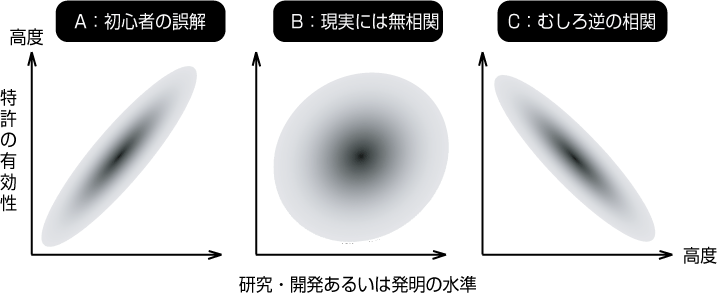
図1.1 発明の水準と特許の有効性
また、包括的で基本的な(ジェネリック)特許は経験を重ね、熟練技術者になれば生まれると考えがちであるが、現実はそうではない。むしろその研究開発に従事した初期に斬新で有力な特許が生まれることが多い。多くの技術者は熟達すればするほど先が見え、その技術の限界を感じる。知らず知らずに自らの創造性を狭くする。それに比べ、初心者は限界を感じないがゆえに、現実の制約を超えた挑戦的な発案をすることがある。その期間の目安は5年である。創造的緊張を維持し、研究的好奇心を保てる平均的な期間と考える。つまり、むしろ若い技術者こそすばらしい特許を生み出すポテンシャルが高いといえるのである。決定的な独創性が要求される数学や理論物理の世界では当たり前なこの事象は特許についても当てはまるといえよう。 <中略>
●第二の目的
第二の目的は第一と対をなすもので、他企業に優位な立場を確立できる有効な特許の権利化には熟達した技が不可欠で強い意志が必要であることを述べる。斬新な発案については若い技術者が優位なことは上に述べた。しかし“良い発明”を淡々と記述するだけでは“良い特許”にはなりえない。斬新で挑戦的な発明をしても、そのままでは磨かれざる原石である。有効な請求範囲を設定できず、また包括的で有用な実施例を提案することができず競合企業の類似製品の発売を阻止できない恐れがある。みすみす大きなビジネスチャンスを失う。特許を仕上げる熟達した技を若い技術者に期待するのは、無理筋である。発案者と特許部門の緊密な連携が必要である。 <中略>
本書は、現実を赤裸々に表したいがため、あえて逆説的な言い方をする場合がある。時には「有力な特許を生むには、高度な研究開発は有効ではない」かの印象を与えかねないが、それは筆者の意図するものではない。あくまで、研究開発に携わってから間もない若い技術者に、思いこみがちな発明や特許の壁を低くし、現実を知った上で自らの特許をよりよくするための手引きであることを忘れないでいただきたい。
また、どんな製品群のどんな段階の研究開発でも、優れた頭脳が徹底的に知恵を絞れば、ニーズからシーズを生み出し、強力な特許が生まれる可能性が高まることを強調したい。優れた頭脳とは、正解があるペーパーテストで高い点数がとれることではない。あふれ出る好奇心と、長く保ち続ける集中力だと筆者は考える。また、このような優れた頭脳が、二人、三人と複数でアイディアを出し合って磨きあえば、包括的でより完成度の高い特許が生まれる。ここに参加して貢献するにはコミュニケーション能力も大事であり、大いにそれを磨いて欲しいと期待する。
I am recommending to apply patents in my book "Patent applicationguide for engineers"(Corona Pub. Co, January 2008)-> for fresh engineers who start research and developmet. My intention written in the preface is as follows.
●Pricipal purpose
A principal purpose of this book is to clear up what beginner engineers are apt to misunderstand for invention and patent. If they do not take adequate lessons for patent, they are likely to think that a level of invention should be that of what Edison did and then they will not able to do it as he did. Furtheremore, they may think that patent should be strong enough to give rise to strong competition between companies leading to spoiling their willingness.
Actual examples are shown in Fig. 1.1. For instance, as shown in Fig. 1.1A, they think that the higher a level of research and development or acamedic performance is, the more powerful its patent is. Thus, they tend to give up to write a strong patent superior to others blaming their poor experience and knowledge. But, actually, the powerfullness of the patent does not correlate with the level of R&D as shown in B, rather a reverse correlation, as shown in C, is shown paradoxically.
The reverse correlation strongly depends on time. A very long time is needed to put academically high-level results to practical use. The effective period of patent is 20 years from its applied time or 15 years form its registered time. Therefore, if the implementation period exceeds those periods, the patent will become invalid. <・・・>
Fig. 1.1 Level of invention and the effectiveness of its patent.
It is thought that only expert engineers with fullof experience can create generic patent however, it is not neccessarily true actually. It is well recognized that novel patent is frequently created in early period when the engineer begins to be engaged in the R&D. The more skillful most of engineers are, the less creative they become. They can well forecast the future thinking of the limits, then they shrink their creativity. On the contrary, since fresh engineers can not estimate the limits they can challenge the breakthrough and create innovtive patents. I think a criterion of the period is 5 years. During 5 years, they can keep inteligent curiosity and a tention for creativity. Thus, rather fresh engineers have a strong potential to create innovative and generic patents. This is very common in fields of mathematics and theoretical physics where absolute creativity is required. This is also common to patent creation. <・・・>
●The second purpose
The second puirpose makes a pair with the principal one. It is described that strong will with expertise is required to win the patent right which is superior to others. It has been already cited above that fresh engineers have an advantage in innovative patent creation. However, simple and plain descriptions can not make a strong patent even if it contains an inovatiove invention. It's like an unpolished ore of diamond. It may not make effective claims with useful applications leading to the loss of effective patent right to rival companies. Consequently, the patgent holder tends to lose business chance. It is unreasonable to require expertise for patent creation to fresh engineers. Close collaboration between an inventorinventor and patent office is inevitable. <・・・>
Paradoxical expressions are sometimes descibed in this book to reveal naked facts. I am afraid that they may give rise to misunderstanding that high-level R&D is not effective to create strong patents. But, it is not my intention. I would like to emphasize that this book is written for fresh engineers who may easily misunderstand that they need very high-level inventions to create patents. This book is a guide for them to get rid of the barrier of the patent creation.
In addition, I would like to emphasize that close collaboration among expert engineersmakes a high-level potential to create strong patents even at any stages of R&D giving birth to seeds from the needs. A superb brain is not that can win a high score in written examination but that can keep concentration and curiosityfro technologies. Whne a few people who hold such brains can make generic and strong inventions and patents. To do that, they need a good communication ability.
特許分割 / Division of patent applied 特許を申請した後、その特許の登録をするためには様々な手続きを経た後に登録されるか却下されるかの裁定が下る。その過程において、他社からその特許を登録させないために異議申し立てという過程がある。申請者はその異議が該当しないとの回答を行わなければならないが、その過程において原特許の記載範囲を逸脱しないように、請求範囲を減縮したり、いくつかの特許に分割することができる。
筆者が行ったトレンチキャパシタセル特許の登録過程における典型的な例を示そう。詳しくは「技術者のための特許事始―半導体技術を中心として」(コロナ社、2008年1月)→ 目次.pdfに記載している。
●最初の出願の請求範囲
最初のトレンチキャパシタ特許:特願昭50-53883「半導体記憶装置」は、下記の請求範囲であった。この申請特許の概念を図2.1に示す。
| 一主表面を有する{110}面とその近傍20度以内の第1導電型半導体基板、該主表面に内側の壁が{111}面とその近傍10度以内の細孔を持ち、該細孔全面あるいはその一部に第2導電型の領域を形成しこれをドレインとし該細孔の第2導電型領域とこれと離間して配設された第2導電型の領域をソースとし、該ソースとドレインの間の上記半導体基板表面上に絶縁膜を介してゲート電極を配設し、上記ドレインと基板の間の接合容量を情報蓄積部とした半導体記憶装置。 |
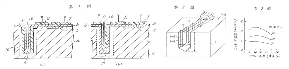
図2.1 最初のトレンチキャパシタセル特許の最初の3図面
本請求範囲には、実質的に致命的に有害な限定が二つ含まれている。特許技術に疎いのにもかかわらず、自分のみで明細書を書き上げた若気の至りである。のちに、“特許技術” というものが確かに存在することを認識することになる。その限定とは、下記の二つである。
(有害な限定-その1) エッチング方法や、基板の方位を限定した→このままだとドライエッチングで(110)以外の面に形成した
細孔キャパシタは含まれない。
(有害な限定-その2) キャパシタを接合容量と限定した→これでは本命のMOSキャパシタが含まれなくなる。
その1は当時、垂直なSi細孔を形成できるドライエッチングが知られていなかったための、限定である(少なくともエッチングの専門家ではなかった筆者は知らなかった)。しかし、幸運なことに、明細書の最後のほうに「細孔を形成する方法を限定しない」という記述を付け加えていたお陰で、最終的にこの限定をはずすことができた。
その2は、これも幸運なことに、自分ではこう限定しながら、<中略>MOSキャパシタの図面を加えていたことから、やはりこの限定をはずすことができた。
審査請求に対して、特許庁からの最初の拒絶理由にはいくつかの公知例が挙げられた。対処した主な二つの先願特許の次に述べる。
●拒絶査定に対する反論
(1) バイポーラトランジスタ+トレンチキャパシタ
その一つは米国T社の先願:特願昭48-61739(昭和48年6月1日)、優先権主張は1972年6月2日(米国)である。この先願は、図2.2に冒頭の図面を示すように、バイポーラトランジスタに溝キャパシタを組み合わせた構造である。構成は酷似しているが、バイポーラであること、「メモリセル」としての使い方には言及していない事を訴えて、退けることができた。 <中略>
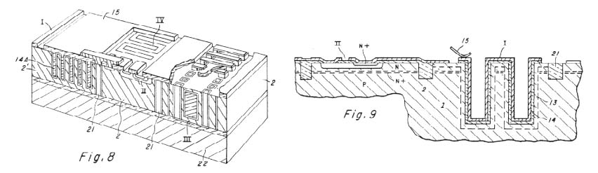
図2.2 トレンチキャパシタ付きバイポーラトランジスタ
(2) 電子回路のコンデンサー
もう一つは、図2.3に示す小型電子回路の薄膜コンデンサーである。従来のコンデンサーは電極の端部が鋭く、電解集中による絶縁破壊を起こしやすいが、基板に丸い穴を形成することによって鋭い端部の発生を抑え、絶縁破壊耐圧を向上させるものである。
これはメモリセルには言及していないが、溝状のコンデンサーという点で、厳しい公知例となった。最終的に、異なる技術であると査定された主な根拠の一つは、明細書に「メモリセルをマトリックス状に配設してメモリーを構成する」というくだりがあり。このマトリックス状という文言が決定的な役割を演じた。図2.4に明細書図面の一部を示す。
半導体メモリである限りマトリックス状に配列するのは当然で、当たり前の技術である。しかし、現実のメモリを実現するには必然的な構成であり、そのような必然性がある構成は、当たり前と思っても明確に記述せよとの教訓である。これも、退けることができた。
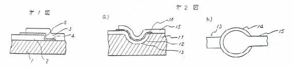
図2.3 公知例その2:小型電子回路の薄膜コンデンサー
図2.4 メモリセルをマトリックス状に配列
●修正した請求範囲
そして、細孔形成条件を削除し、DRAMセルの最小構成要素に限定して、請求範囲を修正した。下記の通りである。
| 情報蓄積部である容量と絶縁ゲート型電界効果型電界効果トランジスタを含んでなる半導体記憶装置において、上記容量は、半導体基板の主表面から上記基板内部に向けて形成された細孔と、該細孔の表面上に積層して形成された絶縁膜および容量電極からなることを特徴とする半導体記憶装置。 |
このように修正できた。これも、「細孔を形成する方法を限定しない」という記述があり、かつ実施例にMOSキャパシタを加えていたのが決定的に役だった。可能な限り実施例を充実せよという教訓である。
●五つに分割した特許
この請求範囲で、特許が公告された。多くの企業から異議が申し立てられ、それらをふまえて、最終的に下記に示すように、原特許は五つに分割された。現在では難しくなっていると聞くが、当時では異議申し立てに伴って比較的容易に分割できたのである。その結果、発明者に大いに有利な請求範囲を設定することができた。
(1) 特願昭58-217716: キャパシタ電極が二つ。
(2) 特願昭58-217717: キャパシタ絶縁膜と駆動トランジスタの絶縁膜が異なる。
(3) 特願昭58-217718: 溝キャパシタと駆動トランジスタがマトリックス状に配列。
(4) 特願昭58-217719: 溝キャパシタ電極をSiで形成。
(5) 特願昭61-104651: 開孔より深い溝のキャパシタ。
集積回路のエキスパートはこれらがどれだけ有効であるかわかるであろう。とくに最後の「開孔より深い溝のキャパシタ」は、現在の主流のDRAMセルであるシリンダ型のスタックキャパシタセルを含むから、この特許は年間世界市場規模が3兆円弱のDRAM全てに適用されていることになる。残念ながら、特許は出願後20年、つまり1995年に失効しているのでロイヤリティは請求できない。もし、クロスライセンス交渉の切り札の一つとして使われていたなら、莫大な貢献をしたことになるが、交渉内容は明らかにされていないから真偽のほどはわからない。
After a patent is applied to the Goverment Patent Office, various kinds of actions are needed for the patent registrtion. After that, a final decision of registration ot rejection is made. Through the process, there is a process of formal rejection(s) by other organization(s). The applicant should reply to them that his patent does meet the objection(s) if he wants to make it awarded. Through the process, he can reduce the original claims and/or divide the original patent into two or more patents so as to keep modified claims within the original ones
Let me show you a typical example of my trench capacitor cell application. Details are described in my book of "Patent application guide for engineers (in Japanese)" (Corona Pub. Co., Jan. 2008)→ contents.pdf.
●Claims in the first application
A claim of the first trench capacitor cell patent of Tokugansho 50-53883, applied in 1975, entitled "Semiconductor memory devices" is as follows. The top 3 figures of the patent are shown in Fig. 2.1. (Note, since the patent was not applied to overseas patents, this claim was not real but virtual.)
| Semiconductor memory device, of which storage portion is a junction capacitance between a drain and a substrate, having a major surface ,of which surface is {110} or within 20 degrees from the {110}, with the first conductivity type and said drain which is formed on a surface of a trench formed on that major surface, of which inner wall is {111} surface or within 20 degrees from the {111} surface; having a source, with the second conductivity type, which is separated with said drain; having a gate electrode whichn is separated by an insulator from said drain and said source. |
Fig. 2.1 Three figures in the first patent application for trench-capacitor cell.
There were two fatal limitations in the original claim. This was because that I made the claim only by myself despite that I was lacking patent expertise. Thjen, I have recognized later there surely exist patent formation techniques. The fatal limitations are as follows.。
(Fatal limitation-A) An etching method and a substrate orientation are limited. Terefore, this claim is not effective to trench capacitor engraved with dry etching.
(Fatal limitation-B) The capacitor is limited to a junction capacitance. Then, major MOS capacitor is not included.
Concerning A, a dry etching method which could engrave vertical trench into the substrate might not availabe available in mid 70's. I was not familiar with dry etching technique anyway. But, very fortuately, I wrote down a description that a method to engrave trenches was not limited to anyone. Therefore, I could delete the limitation concerning an etching method.
Concerning B, fortunately also, even if I limited the capacitor to a junction type, I illustated an MOS capacitor in the descriptions.<・・・> Then I colud also delete the limitation.
Against our request for the examination of the patent, several prior arts were described by the Japanese Patent Office. Major two arts and our action to them are shown below.
●Counterarguments againt rejections of patent office
(1) Prior art-1:Bipolar transistor with a trench capacitor
One of the prior arts was Tokugansho 48-61739 filed on June 1, 1973 inJapan and filed on June 2, 1972 in the US applied from US T-company. As shown in Fig. 2.2, this was a structure of combionation of a bipoklar transistor and a trench capacitor. Despite the structure looked like that of the trench patent, that patent did not refer both to MOS transistor and to memory cell. Thus we aucc succeeded that objection. <・・・>
Fig. 2.2 One prior art: bipolar trasnsistor with a trench capacitor
(2) Prior art-2: Condenser in electric circuits
Another prior art was a thin-film capacitor as shown in Fig. 2.3. A purpose of that patent was to aim at the improvement in dielectric field breakdown by reducing electri-field concentration due to sharp edges of conventional capacitor. This did not refer to memory cell,however this was a strong objection in temrs of trench capacitor.
ppThe major reason why we could avoid this objection was that matrix arrangements of memory cells were written in descriptions as shown in Fig. 2.4. This words of "matrix arrangements" payed a decisive role to avoid the oblection. It is very natural that the matrix arrangement is composed in memory. Even if it is a well-known structure, it should be clearly described it if it is inevitable structure. Thus we succeeded in rejection of the objection. This was a precious experience for us.
Fig. 2.3 Another prior art: A thin film condenser in electric circuits.
Fig. 2.4 Figures of matrix arrangements described in the manuscript opf the patent.
●Revised claims
Finally, the claim was limited to a minimum construction of DRAM cell written below, deleting descriptions related to formation condition of the trench.
In a semiconductor memory device which contains an insulated-gate filed-effect transistor and a capacitor as a strorage element, it features that said capacitor is constructed with a trench extending into major substrate surface and a insulator and an electrode both of which are deposited on wall surface of said. |
Thus, the claim was modified. Descriptions that a method to form the trench was not limited and an application example with MOS capacitor played a decisive role for awarding of the patent. This is a lesson that applications should be enriched as many as possible.
●The first patent divided into 5 ones
ppAfter the patent was notified publicly, many objections were given rise to from a lot of companies. In response to those, the patent was divided into five ones as described below. I have heard that this kind of the division in response to oblections has become difficult today, but it was rather easy at that time, when claims could be modified to be profittable to the applicant.
(#1) Tokugansho 58-217716: Two kinds of capacitor electrodes.
(#2) Tokugansho 58-217717: Two different insulators for a capacitor insulator and a drive transistor.
(#3) Tokugansho 58-217718: Matrix arrangement of trench capacitors and drive transistors.
(#4) Tokugansho 58-217719: Trench capacitor elecrode made by polysilicon.
(#5) Tokugansho 61-104651: Trench capacitor deeper than its opening size.
Expert engineers can easily recognize that these patents are so powerful. Almost all DRAM's must utilize almost all of these. As the last #5 patent includes a cylinder-type stack capacitor cell which is used in major DRAM's today, it is used in all DRAM's to date, of which market volume is around 30 B$ a year. To my deep regret, the patent had already become invalid because 20 years had passed since the date of application of June 1975. If this might has been used as a final bargaining chip at cross-license negotiation, this had contributed to it to a huge extent.
クロスライセンス / Cross license●クロスライセンスとは
最先端産業の分野でしのぎを削っている企業間では、互いに有効な多くの特許を保持していることが多い。このような企業間で互いに特許侵害係争が起こると、平和的な解決手段の一つとして、特許ライセンス交渉が始まる。図3.1に示すように相手企業が侵害していると推定した特許を列挙し、その生産量と価格に一定のライセンス料率をかけて、すべてを積算する。一つの製品に複数の特許を侵害していると推定すると、逐一侵害の内容を判断していかなければならず、かなり複雑なマトリックスで大変な作業量を伴う。典型的な半導体関連のクロスライセンス交渉は次のような性格をもつ。
(1) 半導体では、特許数、製品とも数100件
(2) 全体で10万を超える案件の侵害調査必要
(3) 完全な調査は不可能なので、上からせいぜい数件を審議
(4) 互いの全体金額があまり変わらなければ、包括クロスライセンス、違えば金銭授受
したがって、
(5) 生産額の大きな企業が痛手
(6) 一番怖いのは生産をしない個人の特許(クロスに持ち込む案件がない)
という側面を持つ。
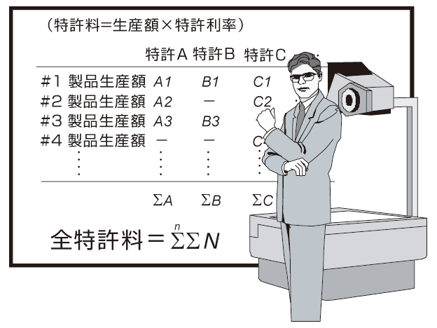
図3.1 クロスライセンス交渉における請求する特許料リストの提示
●クロスライセンスの締結
数百に上った特許の一つ一つを精査することは不可能に近い。それでなくとも紛争が長引けば、特許侵害の疑いのある部品を使っているセットメーカーに迷惑がかかるおそれがあり、両企業の双方にとって得策ではない。そこで、製品ごと、あるいは技術ごとの個別積算額の大きい順に並べて、主なものについてだけ損得勘定をするようである。実際は、数百億円を上回ることもあるらしい。どこまで差があれば、帳尻をあわすために特許料を支払うかは、公にはならない両企業の私的な取り決めによるから、筆者には知るよしもない。
企業間はこのように合意に達すると、互いにクロスライセンスを結び、取り決めによって特許料(ロイヤリティ)を支払うことなく、自由にお互いの特許を使うことができる。特に集積回路のような、複雑で多岐にわたる技術群、製品群が特徴の半導体業界では、大手企業は互いにクロスライセンスを結んでいるようである。
●課題1:独占禁止法に抵触の恐れ
このクロスライセンスには二つの課題がある。一つは、先進企業間でクロスライセンスの輪ができると、新興企業がその輪に入りにくいことになり、独占禁止法に抵触するとの懸念が生じることである。筆者は、法的にどのような議論がされてきたのかは知らないが、懸念が生じるたびに、「疑わしきは罰せず」となってきたと理解している。先進企業が、リソースを投入し、その結果独創的な発明が生じるのは、先進投資の見返りとして当然であるという判断であろうか。また、「世界的に強力な企業の力を弱めることが、国として大いなる損失」であるとしたら、「司法の腕が鈍る」のではないかという懸念を、筆者が何年かに一度必ず感じてきたものである。
●課題2:発明自体の過小評価
もう一つは、発明者の成果が過小に評価されるきらいがあることである。図3.2の上半分に示すように、A、B二社のそれぞれの特許(a)、(b)が、それぞれ他社から100億円の特許料(ロイヤリティ)を受け取れるとしよう。互いに100億円をやりとりすることは、金銭が動かないことと同じであるから、クロスライセンスを結べば、図中下半分に示すように、二つの特許(a)、(b)は、実質的に有効ではないことになる。金銭のやりとりがないことは税法上も得策であるのかもしれない。
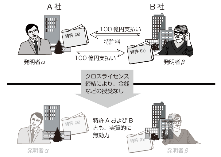
図3.2 クロスライセンスのもう一つに課題 : 発明者の成果が過小評価される。
懸念事項は、発明者に対する有形無形の報償である。有効でない特許に、A社、B社が、それぞれの発明者α、βに相応の報奨を与えるであろうか。もし相応の報奨を与えないとしたら、成果に対する報償として問題はないのであろうか。<中略>、今後優れた技術で市場での地位を上げようとするなら、発明者への報償に対して企業の姿勢を明確にしていかねばならないだろうと思う。
●What is cross license?
Among companies who are competing each other at the forefront of the industry, it is probable that they are holding strongly effective patents each other. When a dispute occurs between two companies on the infringe on patents, they will start a negotiation of cross license as a peaceful means. As shown in Fig. 3.1, they pick up patents on which the opponent is suspected to infringe and then sum up total royalties in terms of output and royalty rate for all products concerned. To win the negotiation, they tend to pick up patents as many as possible. Then, enormous amount of work with complex matrices is given birth to in order to check each validity for each item. A typical negotiation is characterized as follows
(1) Number of products and related patents may exceed several hundrends in semiconductor industry.
(2) Invetigation for more than 100 thousand items on the infringe is sometimes be required.
(3) Thus, a complete investigation looks unreal, therefore several top patents will be argued.
(4) If both summations look almost equivalent, they will conclude a global cross license. If different, one will pay
the balance to another.
Therfore,
(5) One company who is producing a lot than another is has an disadvantage.
(6) The strongest opponent may be an individual who does not produce at all.
Because he does not infringe on any patent.
Fig. 3.1 Presentation of royalty list at cross-license negotiation.
●Conclusion of cross license
It looks impossible to check more than several hundreds of patents concerned. If a negotiation becomes delayed, set makers who are put parts in their products will have troubles to sell them to customers. This will be disadvantageous to both. Terefore, they will pick up several top items in terms of the sum, then they will negotiate each other. It is likely to be rare that the total sum exceeds 1 B$. Since the nogotiation is carried out in strictly confidential manner, nobody outside knows how the negotiation goes.
When companies concerned agree in the negotiation, they conclude a cross license and will use another company's patents without or with pay. Since thre are a lot of complex technologies and very wide variety of products in semiconductor industry, big companies are likely to conclude a treaty on cross license eath other.
●Problem-1: possible violation of antitrust law
There exist two problems for the cross license. Once a cross-license link is settled among advanced companies, new comers are hard to get into the industry. It looks like a violation of antitrust law. I do not know that argument in law world however, I remember they say "suspision alone is not grounds for punishment"everytime the problem occurs. It is understandable that advanced companies have invested a lot to their R&D and then they create innovative inventions and patents as the compensation. If to weaken world strong enterprise will be disadvantageous to them, they may not be strict to the decision. I have been felt every several years.
●Problem-2: :underestimation of invention
Another problem is that the invention and its inventor are likely to be underestimated without an adequate compensation. Provided that a company-A can get 100 M& from another company as a royalty on a patent (a) and vice versa for a company-B on a patent (b), as shown in the upper portion of Fig. 3.2. Consequently they do not pay any to each other with a conclusion of cross license. It may be advantageous on tax law. But, patents (a) and (b) do not look efficient consequently. looks.
Fig. 3.2 Another problem of cross license: underestimation of invention.
A problem is concerned with material and/or immaterial compensations to inventors a and b. Companies A and B may not give adequate compensations to inventors a and b, respectively. Is this a real problem or not? <・・・> To keep or to raise their positions in industry, they should make their attitude clear concerning this issue and offer adequate incentives to employees, I believe.