 |
■研究開発経歴 / R&D History ・ 経歴 / History ・野鳥撮影 / Bird Photograph |
三次元トランジスタ
■三次元トランジスタ研究の動機 ■フィールドシールド・トランジスタ ■ビームチャネル・トランジスタ ■プラズマドーピング ■Siビーム・シリサイド化の新現象 ■自己整合三重ゲートトランジスタ ■自己整合素子分離トランジスタ ■万能セルトランジスタの提案 ■気体絶縁ゲート・トランジスタ |
|
[主要更新 ] '16-11-18: 再構築 '09-2-4:「3-Dトランジスタ」分離 '05-6:原www.suna.cc開設 |
1974年に発表されたシリコンに垂直の溝を形成するエッチング法に触発され、さまざまなアイディアを特許出願した(詳しくは拙書「技術者のための特許事始めー半導体技術を中心として」を参照されたい)。その中に溝の側面をトランジスタのチャネルとして用いるアイディアがいくつかあり、1998年に広島大学ナノデバイス・システム研究センター(現ナノデバイス・バイオ融合科学研究所)に移籍してから昔のアイディの実現を図った。それがここに述べる三次元トランジスタである。アイディアのうち代表的なものを図1および2に示す(なお、特番は特許リストにおける通し番号である)。
当ナノデバイス・システム研究センターは2インチウェハ対応ながら、クラス10のスーパークリーンルーム内に基本的なトランジスタ試作装置はすべてそろっている。その意味では、おそらく世界のどこの大学にも負けないほど充実しているといえよう。実験試作でアイディアを検証することを喜びとしている私にとっては最も望ましい組織である。
●三次元トランジスタの開発課題
三次元トランジスタを開発するにあたり、おもな課題を列挙した。これらに対して10年間をかけて研究を行おうと決めた。それらは、
■■■課題1 : 急峻で原子レベルで平滑な側壁チャネルの形成
■■■課題2 : 側壁に良好に被着されたゲートの形成
■■■課題3 : 側壁への均一な不純物ドーピング
■■■課題4 : 低抵抗な垂直ソース・ドレインの形成
■■■課題5 : 垂直ソース・ドレインへの低接触抵抗電極形成
■■■課題6 : 適切な素子分離構造の提案
■■■課題7 : 優れた自己整合構造をもつトランジスタの提案
である。時系列的にそれぞれを取りあげ、研究を行った。本ページはその記録である。 1999年4月から、学生を2人を指導することになった。大学に赴任後間もないので科研費(科学研究費補助金)などの外部資金を獲得しておらず、高額の製造装置などは購入できない。したがって、ナノデバイス・システム研究センターの装置を利用し、一人の四年生と集積回路の最大課題の一つ、新しい素子分離構造の実現に取り組んだ。
● 集積回路の面積を縮小するのには、(1)トランジスタの縮小、(2)素子分離領域の縮小、そして(3)配線ピッチの縮小が三大要素である。配線ピッチは通常最小加工寸法で決まるので、デバイス開発者にとって工夫のしようがない。トランジスタそれ自身の新たな構造を模索するには時間がなかったので、素子分離領域の縮小を選んだ。実は、集積回路全体を縮小するにはトランジスタの縮小よりは むしろ素子分離領域の縮小のほうが有効である。
●空気分離領域の実現
● 素子分離の主な要件は、
課題A:隣接したデバイス(トランジスタ、キャパシタ、抵抗など)を電気的に分離できること。
要件B: 隣接したデバイス間の物理的距離は短いほど望ましい。
要件C:隣接したデバイス間の寄生静電容量は小さいほど望ましい。
などである。
これらを満たすものとして、デバイス間の分離領域を空気あるいは真空で満たした素子分離を考案し、試作した。 シリコンの溝(トレンチ)に埋め込んだ多結晶シリコンを酸化してフィールド酸化膜を形成するので、活性領域とフィールドシールドの多結晶シリコンおよびフィールド酸化膜の三社が自己整合で形成でき、素子分離領域の縮小が可能となった。
空気分離は比誘電率が1の空気で満たされているから、通常の比誘電率が約4のシリコン酸化膜で満たされている通常の素子分離に比べると寄生容量の値は小さいが、漏洩電界により隣接した接合に影響を与えることがわかった。これは素子分離としては失格である。
そこで、素子分離溝に埋め込んだ多結晶シリコンの上部を酸化することで素子分離溝とフィールド酸化膜を自己整合で形成することを思い付き、実現した。図4にその断面写真をしめす。電気的な素子分離特性も図5に示すように望ましい結果が得られた。
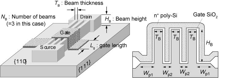
Siの(110)面をTMAH(tetra-methyl-ammonium-hydroxide)溶液でエッチングすると、(111)面のエッチング速度が極端に遅いため、図7に示すような急峻な(111)面壁で構成される垂直のSiビーム(梁)が形成できる。異方性エッチングである。開発当初、これをCCT(corrugated channel transistor)と呼んだ。断面が段ボールのようであるからこう呼んだ(ちなみに段ボールの英名はcorrugated paperである)。
これらのトランジスタはゲート長さが数マイクロメーターと長いものであり、ビーム本数も多いが、さらに微細なビーム幅が40nmのトランジスタ特性を図9と図10に示す。サブスレッショルド特性など、良好なトランジスタ性能を示している。
しかし、図13に示すようなエッジの尖ったパターン部に選択的にArによるスパッタリングが発生して、Si基板が削られた。このスパッタリングによるデバイスへの損傷は顕著で、正常なデバイス特性が得られなかった。また、このスパッタリングは、装置の露出したステンレス部分をスパッタリングし、それがSi基板にドーピングされたことも確認できた。ステンレスの主成分の鉄は、SI中にいわゆる深い不純物レベルを形成し、トランジスタ特性を著しく悪化させることが知られている。
結果から推定すれば、このような平行平板型の装置ではなく、石英のみで囲ったバレル型のほうが汚染を排除する点だけでは望ましかったと言える。また、イオン注入もわずかの傾きで側壁に当てれば反射してある程度下部へも到達することが他の研究機関によって確かめられたので、制約があるとしても汚染がほぼ生じないイオン注入がベターであるといえよう。 しかし、さまざまな現象が見出され、研究の撮り掛としては満足いく結果である。初めからうまくいくことがわかっている研究は、研究ではないとも言えよう。
SiビームをNiシリサイド化すると、図15に示すように幅の厚いビームほど凹凸の激しい形状が得られた。シリサイドが粒成長する際に、供給するシリコンが多いほど粒径も大きくなる。
このシリサイド化の過程で興味ある新現象が観察された。SiがNi膜の粒界に侵入して先に延び、後からNiシリサイドの結晶粒が形成される現象である。その模式図を図16に示した。この新現象のメカニズムを追求したので、トランジスタを試作するまでには至らなかった。このメカニズムについて外部発表している。
このトランジスタの三つのゲートは独立して働くので、三並列接続トランジスタのとなる。図19に特性の一部を示す。サブスレッショルド領域まで独立して制御できることが確かめられた。 これを一つのトランジスタとしてみた場合、他のゲートによって精密のサブスレッショルド電流を制御できるから、多くのトランジスタのサブスレッショルド電流を極限まで精密に合わせることが可能である。作動増幅器の入力段などに適するであろう。
そこで、梁状のシリコンビームを部分的に酸化して、柱状のシリコンピラーと素子分離領域を交互に形成する新しいデバイス構造を考案した。試作して正常な動作をすることを確かめた。
図20は二つのシリコンピラー部と一つのシリコン酸化膜の素子分離領域を示す。このシリコン酸化膜はシリコンビームを部分的にさんかして形成したものであり、当然シリコンピラー部素子分離領域は自己整合で形成されている。実現した構造を図21に示す。シリコンを酸化するとほぼ2倍の厚さのシリコン酸化膜が径背される。しかし、図21に示した状態では、シリコンピラーより酸化膜のほうが薄いが、これはさまざまな酸化膜エッチング処理により酸化膜が選択的に薄くなった結果である。
図20に示した構造からわかるように、一本のシリコンピラーの左右に独立した二つのチャネルが形成できる。図22に二つのトランジスタが独立に制御できることを示す。
このトランジスタを実現するに当たりさまざまな障害があった。いかにゲート下の絶縁膜を除去するか、ゲートに高電圧が印加された場合、他の部分で絶縁破壊しないための構造をどうするかなどである。それらに対処した構造を図24にしめす。また、実現したゲート下の断面図を図25にしめした。
ゲートに印加した電圧を徐々に上昇した場合のゲートのリーク電流を図26に示す。MOSトランジスタは30数Vで破壊したのち、ゲートが低抵抗で基板と接続されたが、MGSトランジスタは30V程度で絶縁破壊したのちは、むしろ耐圧が上がっている。弱い部分が消滅したからであろう。 ただし、この強い強制破壊はトランジスタそのものを破壊したので、高耐圧の意味がない。さらに弱い強制破壊や、耐放射線、ホットキャリヤ耐性などを測定する必要がある。
●Developmet subjects of 3-D transistors
When I started to develop 3-D transistors, I have chosen major subjects for coming 10 years. They are,
■■■subject 1 : formation of steep and atomically-flat siewall channels,
■■■subject 2 : formation of conformal gate on sidewalls,
■■■subject 3 : uniform impurityn doping to sidewalls,
■■■subject 4 : formation of low-resistive vertical source and drain, and
■■■subject 5 : formation of low-resistive contacts to vertical source and drain.
■They have been developed sequentially during these 10 years since 1998. They are described in this page.
Parasitic capacitance of air isolation, as shown in Fig. 3(b), is smaller than that of conventional SiO2 isolation because specific permittivity of air is 1 while that of SiO2 is about 4. But it was found thatleakage electric field gave strong effect to ajacent deivesstrongly influences. Ths, we stopped persuing its development.
Then, we got an idea of field-shield isolation described above. Cross sections of the field-shield isolation structure is shown in Fig. 4 and satisfactory electrical isolation performance is shown in Fig. 5.
<Publication>
1) A. Takase, T. Kidera, and H. Sunami, “Field-Shield Trench Isolation with Self-Aligned Field Oxide,” Extended Abstracts of International Symp. on Solid State Devices and Materials, Abs. No. A-7-4, pp. 694-695, Nagoya, Sept. 17-19, 2002.
2) A. Takase, T. Kidera, and H. Sunami, “Field-Shield Trench Isolation with Self-Aligned Field Oxide,” Jpn. J. Appl. Phys., Vol. 42, Part 1, No. 4B, pp. 2100-2105, April 2003.
These transistors had long channels of longer than several micrometers and number of beams were many. Subseqently, we developed much smaller beam-channel transistor of which beam width is 40 nm, as shown in Fig. 9. Satisfactory subthreshold characteristecs were observed.
<Publication>
3) T. Furukawa, H. Yamashita, and H. Sunami, “Corrugated-Channel Transistor (CCT) for Area-Conscious Applications,” Extended Abstracts of International Symp. on Solid State Devices and Materials, Abs. No. A-3-2, pp. 139-140, Nagoya, Sept. 17-19, 2002.
4) T. Furukawa, H. Yamashita, and H. Sunami, “A Proposal of Corrugated-Channel Transistor (CCT) with Vertically-Formed Channels for Area-Conscious Applications,” Jpn. J. Appl. Phys., Vol. 42, Part 1, No. 4B, pp. 2067-2072, April 2003.
5) A. Katakami, K. Kobayashi, and H. Sunami, “High-Aspect Ratio gate Formation of Beam-Channel MOS Transistor with Impurity-Enhanced oxidation of Silicon Gate,” Extended Abstracts of International Symp. on Solid State Devices and Materials, Abs. No. D-5-2, pp. 282-283, Tokyo, Sept. 16-18, 2003.
6) A. Katakami, K. Kobayashi, and H. Sunami, “A High-Aspect Ratio Silicon Gate Formation Technique for Beam-Channel MOS Transistor with Impurity-Enhanced Oxidation,” Jpn. J. Appl. Phys., Vol. 43, No. 4B, pp. 2145-2150, April 2004.
7) H. Sunami, T. Furukawa, and T. Masuda, “A Three-Dimensional MOS Transistor Formation Technique with Crystallographic Orientation-Dependent TMAH Etchant,” SENSORS and ACTUATORS A: PHYSICAL, A111, pp. 310-316, 2004.
Curious phenomena were found that Si atoms penetrated into Ni film along Ni grain boundaries, then Ni-silicide grains were formed. A model of this mechanism is shown in Fig. 16. Persuing this mechanism did not provide us enough time to fabricate 3-D transistors with silicided source and drain. This mechanism was published.
<Publication>
11) S. Matsumura, A. Sugimura, K. Okuyama, and H. Sunami, “Anomalous Whisker Generation in Ni-Silicided Source and Drain for Three-Dimensional Beam-Channel MOS Transistor on SOI Substrate,” Abstract of Advanced Metallization Conference, pp. 90-91, Sept. 25-27, Tokyo, 2006.
12) Shunpei Matsumura, Atsushi Sugimura, Kiyoshi Okuyama, and Hideo Sunami, “Anomalous Whisker Generation in Ni-Silicided Source and Drain for Three-Dimensional Beam-Channel MOS Transistor on SOI Substrate,” Proc. of Advanced Metallization Conference 2006, pp. 631-635, ADMETA, 2007.
13) Kiyoshi. Okuyama, Atsushi. Sugimura, and Hideo. Sunami, “An Optimized Silicidation Technique for Source and Drain of FINFET,” Extended Abstracts of International Symp. on Solid State Devices and Materials, pp. 1044-1045, Tokyo, Sept. 19-21, 2007.
14) Kiyoshi Okuyama, Atsushi Sugimura, and Hideo Sunami, “Optimized Silicidation Technique for Source and Drain of Fin-Type Field-Effect Transistor,” Jpn. J. Appl. Phys., Vol. 47, No. 4, pp. 2407-2409, 2008.
As these three transistor can be operated independently, three-parallel transistor scheme is obtained. A part of their performance is shown in Fig. 19. Satisfactory perfprmance is shown in subthreshold region. Looking at three transistors as one transistor, subthreshold characteristics of a lot of transistors can be precisely tuned so that absolutely the same subthresholf performance. They may be suitable input transistors of a differential amplifier.
<Publiaction>
15) K. Okuyama, K. Yoshikawa, and H. Sunami, “Characterization of Subthreshold Behavior of Narrow-Channel SOI nMOSFET with Additional Side-Gate Electrodes,” Extended Abstracts of International Symp. on Solid State Devices and Materials, pp. 506-507, Tokyo, Sept. 13-15, 2006.
16) K. Okuyama, K. Yoshikawa, and H. Sunami, “Control of Subthreshold-Characteristics of Narrow- channel SOI nMOS Transistor Utilized Additional Side Gate Electrodes,” Jpn. J. Appl. Phys., Vol. 46, No. 4B, pp. 2050-2053, 2007.
17) K. Okuyama, K. Yoshikawa, and H. Sunami “Proposal of 3-Dimensional Independent Triple-Gate MOS Transistor with Dynamic Current Control,” 14th International Symposium on VLSI Technology, Systems, and Applications (2007 VLSI-TSA), Hsinchu, Taiwan, April 23-25, 2007.
Figure 20 shows an alternate structures of silicon pillar and silicon dioxide pillar which is transformed from silicon pillar itself. Therefore, two kinds of pillars are formed in self-aligned manner. One of realized structure is shown in Fig. 21. The thickness of silicon dioxide is almost twice as much as that of silicon which is to be converted into the silicon dioxide. However, the thickness of the silikcon dioxide is a little bit thinner than that of the silicon. This is because the silicon dioxide is thined by subsequent several etching processes.
As shown in Fig. 20, two independent channels are formed at both sidewalls of a pillar. This is evident in Fig. 22.
<Publication>
18) Atsushi Sugimura, Kiyoshi Okuyama, and Hideo Sunami, “A Vertical-Channel Metal-Oxide- Semiconductor Field-Effect Transistor with Fully-Oxidized Silicon Beam Isolation,” Extended Abstracts of International Symp. on Solid State Devices and Materials, P-3-8, pp. 418-419, Tsukuba, Sept. 23-26, 2008.
19) Hideo Sunami, “Development of three-dimensional MOS structures from trench-capacitor DRAM cell to pillar-type transistor,” Proc. the 9th International Conference on Solid-State and Integrated- Circuit Technology, Abs. No. D2.2, pp. 853-856, Beijin, China, October 20-23, 2008.
10) Atsushi Sugimura, Kiyoshi Okumura, Hideo Sunami, “Proposal of a Vertical-Channel Metal Oxide Semiconductor Field-Effect Transistor with Entirely Oxidized Silicon Beam Isolation,” Metal-Oxide- Semiconductor Silicon Optical Modulator Based on Inversion-Carrier Absorption,” Jpn. J. Appl. Phys., Vol. 48, No. 4, pp. 04C049-1-4, 2009.
Gate leakage currents are shown in Fig. 26 before and after forced catastrophic breakdown of gate insulator. Gate shortage occurred after high lamp voltage in conventional MOS transistor, otherwise, gate insulation became better than before in MGS transistor. It is speculated that weak portions were blown away in MGS.
But this forced breakdown procedure also broke transistor itself. It is senseless. We should evaluate radiation hardness, hot-carrier immunity as well as weaker forced breakdown procedure.
<Publication>
22) Youichi Ashida, Kiyoshi Okuyama, and Hideo Sunami, “Proposal of a metal-gas-semiconductor field-effect transistor, MGSFET with potential catastrophic-breakdown hardness,” Abstract of 34th International Conference on Micro and Nano Engineering, Abs. No. NED-P16, Athens, Greece, Sept. 15-18, 2008.
当ナノデバイス・システム研究センターは2インチウェハ対応ながら、クラス10のスーパークリーンルーム内に基本的なトランジスタ試作装置はすべてそろっている。その意味では、おそらく世界のどこの大学にも負けないほど充実しているといえよう。実験試作でアイディアを検証することを喜びとしている私にとっては最も望ましい組織である。
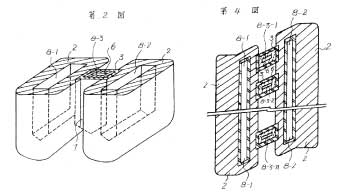 図1 基板に掘り込んだ溝の側壁をチャネルとした三次元 MOSトランジスタ(1975年出願/特番40) |
 図2 自己整合三重ゲート三次元トランジスタ(1983年出願/特番138) |
三次元トランジスタを開発するにあたり、おもな課題を列挙した。これらに対して10年間をかけて研究を行おうと決めた。それらは、
■■■課題1 : 急峻で原子レベルで平滑な側壁チャネルの形成
■■■課題2 : 側壁に良好に被着されたゲートの形成
■■■課題3 : 側壁への均一な不純物ドーピング
■■■課題4 : 低抵抗な垂直ソース・ドレインの形成
■■■課題5 : 垂直ソース・ドレインへの低接触抵抗電極形成
■■■課題6 : 適切な素子分離構造の提案
■■■課題7 : 優れた自己整合構造をもつトランジスタの提案
である。時系列的にそれぞれを取りあげ、研究を行った。本ページはその記録である。 1999年4月から、学生を2人を指導することになった。大学に赴任後間もないので科研費(科学研究費補助金)などの外部資金を獲得しておらず、高額の製造装置などは購入できない。したがって、ナノデバイス・システム研究センターの装置を利用し、一人の四年生と集積回路の最大課題の一つ、新しい素子分離構造の実現に取り組んだ。
● 集積回路の面積を縮小するのには、(1)トランジスタの縮小、(2)素子分離領域の縮小、そして(3)配線ピッチの縮小が三大要素である。配線ピッチは通常最小加工寸法で決まるので、デバイス開発者にとって工夫のしようがない。トランジスタそれ自身の新たな構造を模索するには時間がなかったので、素子分離領域の縮小を選んだ。実は、集積回路全体を縮小するにはトランジスタの縮小よりは むしろ素子分離領域の縮小のほうが有効である。
●空気分離領域の実現
● 素子分離の主な要件は、
課題A:隣接したデバイス(トランジスタ、キャパシタ、抵抗など)を電気的に分離できること。
要件B: 隣接したデバイス間の物理的距離は短いほど望ましい。
要件C:隣接したデバイス間の寄生静電容量は小さいほど望ましい。
などである。
これらを満たすものとして、デバイス間の分離領域を空気あるいは真空で満たした素子分離を考案し、試作した。 シリコンの溝(トレンチ)に埋め込んだ多結晶シリコンを酸化してフィールド酸化膜を形成するので、活性領域とフィールドシールドの多結晶シリコンおよびフィールド酸化膜の三社が自己整合で形成でき、素子分離領域の縮小が可能となった。
 (a) 多結晶Si埋設 (b) 空気充填 図3 二様の素子分離 |
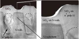 図4 フィールドシールド素子分離 |
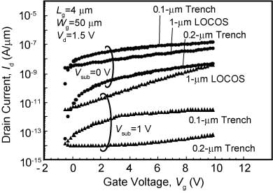 図5 LOCOSとフィールドシールドが分離電流に与える影響 |
空気分離は比誘電率が1の空気で満たされているから、通常の比誘電率が約4のシリコン酸化膜で満たされている通常の素子分離に比べると寄生容量の値は小さいが、漏洩電界により隣接した接合に影響を与えることがわかった。これは素子分離としては失格である。
そこで、素子分離溝に埋め込んだ多結晶シリコンの上部を酸化することで素子分離溝とフィールド酸化膜を自己整合で形成することを思い付き、実現した。図4にその断面写真をしめす。電気的な素子分離特性も図5に示すように望ましい結果が得られた。
<外部発表>
1) A. Takase, T. Kidera, and H. Sunami, “Field-Shield Trench Isolation with Self-Aligned Field Oxide,” Extended Abstracts of International Symp. on Solid State Devices and Materials, Abs. No. A-7-4, pp. 694-695, Nagoya, Sept. 17-19, 2002.
2) A. Takase, T. Kidera, and H. Sunami, “Field-Shield Trench Isolation with Self-Aligned Field Oxide,” Jpn. J. Appl. Phys., Vol. 42, Part 1, No. 4B, pp. 2100-2105, April 2003.
Siの(110)面をTMAH(tetra-methyl-ammonium-hydroxide)溶液でエッチングすると、(111)面のエッチング速度が極端に遅いため、図7に示すような急峻な(111)面壁で構成される垂直のSiビーム(梁)が形成できる。異方性エッチングである。開発当初、これをCCT(corrugated channel transistor)と呼んだ。断面が段ボールのようであるからこう呼んだ(ちなみに段ボールの英名はcorrugated paperである)。
 (a) 鳥瞰図 (b) 断面図 図6 Siビームトランジスタ |
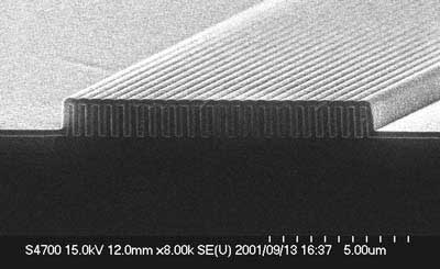 図7 多結晶Siで覆われた31本のSiビーム |
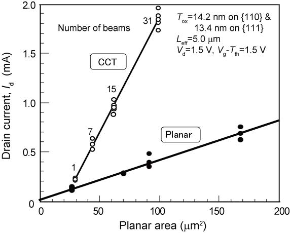 図8 平面トランジスタとの比較 |
これらのトランジスタはゲート長さが数マイクロメーターと長いものであり、ビーム本数も多いが、さらに微細なビーム幅が40nmのトランジスタ特性を図9と図10に示す。サブスレッショルド特性など、良好なトランジスタ性能を示している。
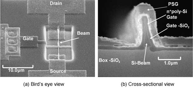 図9 ビームチャネル・トランジスタ |
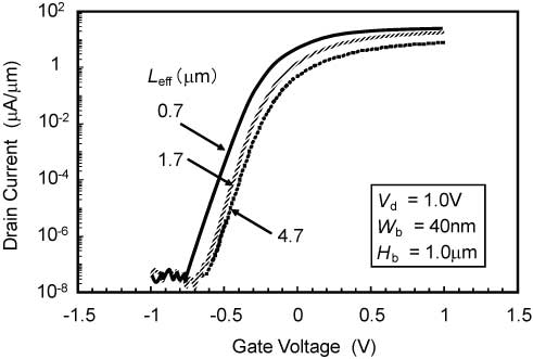 図10 ドレイン電流ー ゲート電圧特性 |
<外部発表>
3) T. Furukawa, H. Yamashita, and H. Sunami, “Corrugated-Channel Transistor (CCT) for Area-Conscious Applications,” Extended Abstracts of International Symp. on Solid State Devices and Materials, Abs. No. A-3-2, pp. 139-140, Nagoya, Sept. 17-19, 2002.
4) T. Furukawa, H. Yamashita,?and H. Sunami, “A Proposal of Corrugated-Channel Transistor (CCT) with Vertically-Formed Channels for Area-Conscious Applications,” Jpn. J. Appl. Phys., Vol. 42, Part 1, No. 4B, pp. 2067-2072, April 2003.
5) A. Katakami, K. Kobayashi, and H. Sunami, “High-Aspect Ratio gate Formation of Beam-Channel MOS Transistor with Impurity-Enhanced oxidation of Silicon Gate,” Extended Abstracts of International Symp. on Solid State Devices and Materials, Abs. No. D-5-2, pp. 282-283, Tokyo, Sept. 16-18, 2003.
6) A. Katakami, K. Kobayashi, and H. Sunami, “A High-Aspect Ratio Silicon Gate Formation Technique for Beam-Channel MOS Transistor with Impurity-Enhanced Oxidation,” Jpn. J. Appl. Phys., Vol. 43, No. 4B, pp. 2145-2150, April 2004.
7) H. Sunami, T. Furukawa, and T. Masuda, “A Three-Dimensional MOS Transistor Formation Technique with Crystallographic Orientation-Dependent TMAH Etchant,” SENSORS and ACTUATORS A: PHYSICAL, A111, pp. 310-316, 2004.
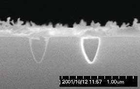
しかし、図13に示すようなエッジの尖ったパターン部に選択的にArによるスパッタリングが発生して、Si基板が削られた。このスパッタリングによるデバイスへの損傷は顕著で、正常なデバイス特性が得られなかった。また、このスパッタリングは、装置の露出したステンレス部分をスパッタリングし、それがSi基板にドーピングされたことも確認できた。ステンレスの主成分の鉄は、SI中にいわゆる深い不純物レベルを形成し、トランジスタ特性を著しく悪化させることが知られている。
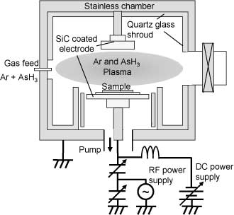 図11 プラズマドーピング装置 |
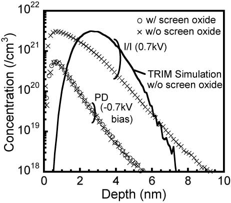 図12 ドープされたAsの分布 |
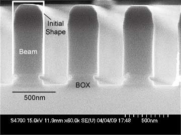 図13 スパッタによって削られた表面 |
結果から推定すれば、このような平行平板型の装置ではなく、石英のみで囲ったバレル型のほうが汚染を排除する点だけでは望ましかったと言える。また、イオン注入もわずかの傾きで側壁に当てれば反射してある程度下部へも到達することが他の研究機関によって確かめられたので、制約があるとしても汚染がほぼ生じないイオン注入がベターであるといえよう。 しかし、さまざまな現象が見出され、研究の撮り掛としては満足いく結果である。初めからうまくいくことがわかっている研究は、研究ではないとも言えよう。
<外部発表>
8) K. Kobayashi, T. Eto, K. Okuyama, K. Shibahara, and H. Sunami, “An Impurity-Enhanced Oxidation Assisted Doping Profile Evaluation for Three-Dimensional and Vertical-Channel Transistors,” Extended Abstracts of International Symp. on Solid State Devices and Materials, Abs. No. B-6-3, pp. 208-209, Tokyo, Sept. 15-17, 2004.
9) K. Kobayashi, T. Eto, K. Okuyama, K. Shibahara, and H. Sunami, “Application of Arsenic Plasma Doping in Three-Dimensional MOS Transistors and the Doping Profile Evaluation,” Jpn. J. Appl. Phys., Vol. 44, No. 4B, pp. 2273-2278, April 2005.
10) Kei Kobayashi, Kiyoshi Okuyama, and Hideo Sunami, “Plasma doping induced damages associated with source/drain fomrmation in three-dimensional beam-channel MOS transistor,” Microelectronic Engineering, Vol. 84, pp. 1631-1634, 2007.
SiビームをNiシリサイド化すると、図15に示すように幅の厚いビームほど凹凸の激しい形状が得られた。シリサイドが粒成長する際に、供給するシリコンが多いほど粒径も大きくなる。
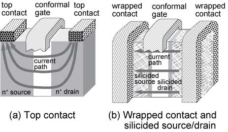 図14 シリサイド・ソース/ドレインの特長 |
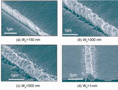 図15 Niシリサイド化したSiビーム |
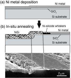 図16 Niシリサイドの這い上がり現象 |
このシリサイド化の過程で興味ある新現象が観察された。SiがNi膜の粒界に侵入して先に延び、後からNiシリサイドの結晶粒が形成される現象である。その模式図を図16に示した。この新現象のメカニズムを追求したので、トランジスタを試作するまでには至らなかった。このメカニズムについて外部発表している。
<外部発表>
11) S. Matsumura, A. Sugimura, K. Okuyama, and H. Sunami, “Anomalous Whisker Generation in Ni-Silicided Source and Drain for Three-Dimensional Beam-Channel MOS Transistor on SOI Substrate,” Abstract of Advanced Metallization Conference, pp. 90-91, Sept. 25-27, Tokyo, 2006.
12) Shunpei Matsumura, Atsushi Sugimura, Kiyoshi Okuyama, and Hideo Sunami, “Anomalous Whisker Generation in Ni-Silicided Source and Drain for Three-Dimensional Beam-Channel MOS Transistor on SOI Substrate,” Proc. of Advanced Metallization Conference 2006, pp. 631-635, ADMETA, 2007.
13) Kiyoshi. Okuyama, Atsushi. Sugimura, and Hideo. Sunami, “An Optimized Silicidation Technique for Source and Drain of FINFET,” Extended Abstracts of International Symp. on Solid State Devices and Materials, pp. 1044-1045, Tokyo, Sept. 19-21, 2007.
14) Kiyoshi Okuyama, Atsushi Sugimura, and Hideo Sunami, “Optimized Silicidation Technique for Source and Drain of Fin-Type Field-Effect Transistor,” Jpn. J. Appl. Phys., Vol. 47, No. 4, pp. 2407-2409, 2008.
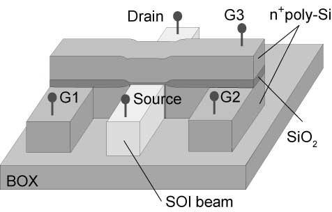 図17 超自己整合三重ゲートトランジスタ |
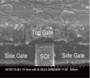 図18 実現した構造 |
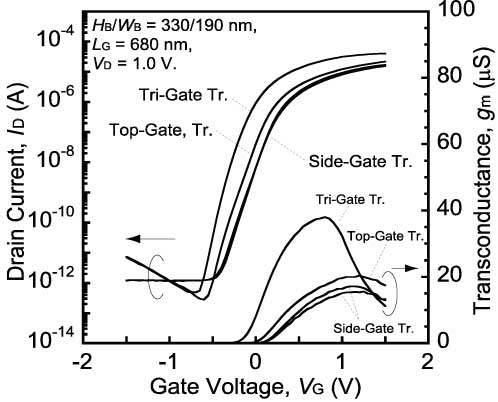 図19 実現したトランジスタ特性 |
このトランジスタの三つのゲートは独立して働くので、三並列接続トランジスタのとなる。図19に特性の一部を示す。サブスレッショルド領域まで独立して制御できることが確かめられた。 これを一つのトランジスタとしてみた場合、他のゲートによって精密のサブスレッショルド電流を制御できるから、多くのトランジスタのサブスレッショルド電流を極限まで精密に合わせることが可能である。作動増幅器の入力段などに適するであろう。
<外部発表>
15) K. Okuyama, K. Yoshikawa, and H. Sunami, “Characterization of Subthreshold Behavior of Narrow-Channel SOI nMOSFET with Additional Side-Gate Electrodes,” Extended Abstracts of International Symp. on Solid State Devices and Materials, pp. 506-507, Tokyo, Sept. 13-15, 2006.
16) K. Okuyama, K. Yoshikawa, and H. Sunami, “Control of Subthreshold-Characteristics of Narrow- channel SOI nMOS Transistor Utilized Additional Side Gate Electrodes,” Jpn. J. Appl. Phys., Vol. 46, No. 4B, pp. 2050-2053, 2007.
17) K. Okuyama, K. Yoshikawa, and H. Sunami “Proposal of 3-Dimensional Independent Triple-Gate MOS Transistor with Dynamic Current Control,” 14th International Symposium on VLSI Technology, Systems, and Applications (2007 VLSI-TSA), Hsinchu, Taiwan, April 23-25, 2007.
そこで、梁状のシリコンビームを部分的に酸化して、柱状のシリコンピラーと素子分離領域を交互に形成する新しいデバイス構造を考案した。試作して正常な動作をすることを確かめた。
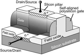 図20 超自己整合素子分離トランジスタ |
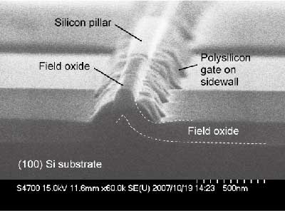 図21 実現した構造 |
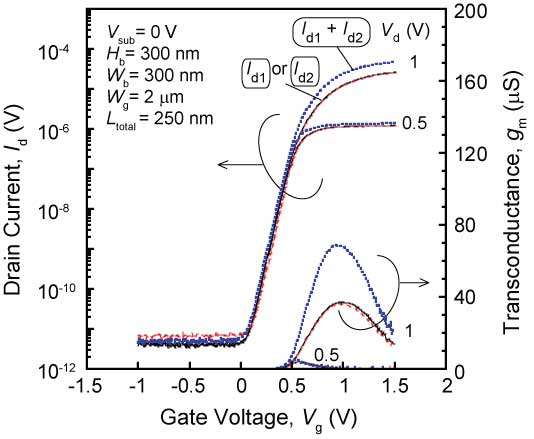 図22 実現したトランジスタ特性 |
図20は二つのシリコンピラー部と一つのシリコン酸化膜の素子分離領域を示す。このシリコン酸化膜はシリコンビームを部分的にさんかして形成したものであり、当然シリコンピラー部素子分離領域は自己整合で形成されている。実現した構造を図21に示す。シリコンを酸化するとほぼ2倍の厚さのシリコン酸化膜が径背される。しかし、図21に示した状態では、シリコンピラーより酸化膜のほうが薄いが、これはさまざまな酸化膜エッチング処理により酸化膜が選択的に薄くなった結果である。
図20に示した構造からわかるように、一本のシリコンピラーの左右に独立した二つのチャネルが形成できる。図22に二つのトランジスタが独立に制御できることを示す。
<外部発表>
18) Atsushi Sugimura, Kiyoshi Okuyama, and Hideo Sunami, “A Vertical-Channel Metal-Oxide- Semiconductor Field-Effect Transistor with Fully-Oxidized Silicon Beam Isolation,” Extended Abstracts of International Symp. on Solid State Devices and Materials, P-3-8, pp. 418-419, Tsukuba, Sept. 23-26, 2008.
19) Hideo Sunami, “Development of three-dimensional MOS structures from trench-capacitor DRAM cell to pillar-type transistor,” Proc. the 9th International Conference on Solid-State and Integrated- Circuit Technology, Abs. No. D2.2, pp. 853-856, Beijin, China, October 20-23, 2008.
20) Atsushi Sugimura, Kiyoshi Okumura, Hideo Sunami, “Proposal of a Vertical-Channel Metal Oxide Semiconductor Field-Effect Transistor with Entirely Oxidized Silicon Beam Isolation,” Metal-Oxide- Semiconductor Silicon Optical Modulator Based on Inversion-Carrier Absorption,” Jpn. J. Appl. Phys., Vol. 48, No. 4, pp. 04C049-1-4, 2009.
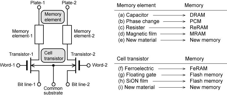 図23 提案した万能セルトランジスタ構成 |
<外部発表>
21) Hideo Sunami, "Dimension Increase in Metal-Oxide-Semiconductor Memories and Transistors," to be published IN-TECH.
21) Hideo Sunami, "Dimension Increase in Metal-Oxide-Semiconductor Memories and Transistors," to be published IN-TECH.
このトランジスタを実現するに当たりさまざまな障害があった。いかにゲート下の絶縁膜を除去するか、ゲートに高電圧が印加された場合、他の部分で絶縁破壊しないための構造をどうするかなどである。それらに対処した構造を図24にしめす。また、実現したゲート下の断面図を図25にしめした。
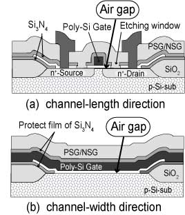 図24 ゲート周辺断面構造 |
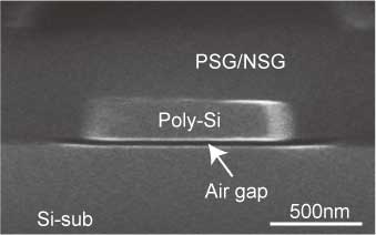 図25 実現したゲート断面 |
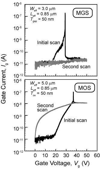 図26 強制破壊前後のゲートリーク電流 |
ゲートに印加した電圧を徐々に上昇した場合のゲートのリーク電流を図26に示す。MOSトランジスタは30数Vで破壊したのち、ゲートが低抵抗で基板と接続されたが、MGSトランジスタは30V程度で絶縁破壊したのちは、むしろ耐圧が上がっている。弱い部分が消滅したからであろう。 ただし、この強い強制破壊はトランジスタそのものを破壊したので、高耐圧の意味がない。さらに弱い強制破壊や、耐放射線、ホットキャリヤ耐性などを測定する必要がある。
<外部発表>
22) Youichi Ashida, Kiyoshi Okuyama, and Hideo Sunami, “Proposal of a metal-gas-semiconductor field-effect transistor, MGSFET with potential catastrophic-breakdown hardness,” Abstract of 34th International Conference on Micro and Nano Engineering, Abs. No. NED-P16, Athens, Greece, Sept. 15-18, 2008.
22) Youichi Ashida, Kiyoshi Okuyama, and Hideo Sunami, “Proposal of a metal-gas-semiconductor field-effect transistor, MGSFET with potential catastrophic-breakdown hardness,” Abstract of 34th International Conference on Micro and Nano Engineering, Abs. No. NED-P16, Athens, Greece, Sept. 15-18, 2008.
■ Being stimulated with an etching method which makes steep vertical silicon trenches published in 1974, I have applied various patents. Details are shown in a book of "Patent appilication guide for engineers". Several ideas out of them claim that trench walls are utilized as transistor channels. After I moved to Reserch Center for Nanodevices and Systems, Hiroshima University in 1998, I began to implement those ideas. They were three-dimensional (3-D) transistors. Some of them are shown in Figs. 1 and 2. Patent serial number, Pat# is connected to that described in patent list.
This research center provides almost all apparatus in super clean room of class 10 to fabricate fundamental MOS transistors even if wafer size is 2 inches in diameter. As one of clean room facilities in universities, this center's facilities are undoubtedly among the top class in the world. Wanting to implement my device ideas, I recognized that they were adequately available for possible fabrication of advanced CMOS devices.
This research center provides almost all apparatus in super clean room of class 10 to fabricate fundamental MOS transistors even if wafer size is 2 inches in diameter. As one of clean room facilities in universities, this center's facilities are undoubtedly among the top class in the world. Wanting to implement my device ideas, I recognized that they were adequately available for possible fabrication of advanced CMOS devices.
Fig. 1 3-D MOS transistor of which channels are formed inside trenches. (appled in 1975/Pat#40) |
Fig. 2 Self-aligned, triple gate, 3-D transistors (appled in 1983/Pat #138) |
●Developmet subjects of 3-D transistors
When I started to develop 3-D transistors, I have chosen major subjects for coming 10 years. They are,
■■■subject 1 : formation of steep and atomically-flat siewall channels,
■■■subject 2 : formation of conformal gate on sidewalls,
■■■subject 3 : uniform impurityn doping to sidewalls,
■■■subject 4 : formation of low-resistive vertical source and drain, and
■■■subject 5 : formation of low-resistive contacts to vertical source and drain.
■They have been developed sequentially during these 10 years since 1998. They are described in this page.
● I began to guide two 4-th grade students in April 1999. Due to limited time from when I got this post at Hiroshima university, I did not get any Grand-in Aid for Scientific Research from Japanese government. Therefore, I could not buy an expensive apparatus to carry out our research. Utilizing existing equipment here, Research Center for Nanodevices and Systems, we started a research on new isolation technique as one of the most important subjects of integrated circuits.
● To reduce the area of integrated circuits, major three factors exist such as (1) reduction of transistor size, (2) reduction of isolation region, and (3) decrease in metallization pitch. Since the metallization pitch is defined by minimum feature size, there is few subjects for device developers. While, we could not set a new idea at that time for the transistor structure itself, we have chosen the reduction of isolation region. It was more efficient to reduce entire area of integrated circuit than area reduction of transistor itself.
●Development of air isolation
● Major factors to make an adequate isolation structure are
(1) electrical separation between ajacent devices such as transistor, capacitor, and resister,
(2) physically short isolationn region, and
(3) small parasitic capacitance between ajacent devices.
● To satisfy these factors, we proposed an air isolation structure and successfully implemented it Since field oxide is transformed from polysilicon which is buried into silicon trench, three strucutes of active region, field shield of polysilicon, and field oxide are formed in self-aligned manner leading to smaller isolation region.
(a) buried poly-Si (b) air Fig. 3 Two kinds of isolation., |
Fig. 4 Proposed field-shield isolation structure. |
Fig. 5 Influences of LOCOS and trench on isolation. |
Parasitic capacitance of air isolation, as shown in Fig. 3(b), is smaller than that of conventional SiO2 isolation because specific permittivity of air is 1 while that of SiO2 is about 4. But it was found thatleakage electric field gave strong effect to ajacent deivesstrongly influences. Ths, we stopped persuing its development.
Then, we got an idea of field-shield isolation described above. Cross sections of the field-shield isolation structure is shown in Fig. 4 and satisfactory electrical isolation performance is shown in Fig. 5.
<Publication>
1) A. Takase, T. Kidera, and H. Sunami, “Field-Shield Trench Isolation with Self-Aligned Field Oxide,” Extended Abstracts of International Symp. on Solid State Devices and Materials, Abs. No. A-7-4, pp. 694-695, Nagoya, Sept. 17-19, 2002.
2) A. Takase, T. Kidera, and H. Sunami, “Field-Shield Trench Isolation with Self-Aligned Field Oxide,” Jpn. J. Appl. Phys., Vol. 42, Part 1, No. 4B, pp. 2100-2105, April 2003.
● I and another 4-th garde student began research on Si optical modulator in April 1999 (refer to "Si optical mudulator"in details). As This modulator strucute was absolutely a 3-D transistor which had plural vertical channels resulting in successful implementation of the 3-D transistor as shown in Fig. 6.
We can get steep and vertical walls of (111) crystal orientation when we use (110) single crystal silicon. Because, an etch rate of (111) is much slower than that of any other crystal orientations. We call this kind of etchig "anisotropic etchig." When we succeedded in development of this transistor, we named it "corrugated channel transistor, CCT". Its channels looked like a cross section of corrugated paper.
We can get steep and vertical walls of (111) crystal orientation when we use (110) single crystal silicon. Because, an etch rate of (111) is much slower than that of any other crystal orientations. We call this kind of etchig "anisotropic etchig." When we succeedded in development of this transistor, we named it "corrugated channel transistor, CCT". Its channels looked like a cross section of corrugated paper.
(a) Bird’s eye view (b) Cross-section Fig. 6 Silicon beam transistor |
Fig.7 Polysilicon covered 31 Si beams |
Fig. 8 Performance comparison with planar transistor |
These transistors had long channels of longer than several micrometers and number of beams were many. Subseqently, we developed much smaller beam-channel transistor of which beam width is 40 nm, as shown in Fig. 9. Satisfactory subthreshold characteristecs were observed.
Fig. 9 Realized beam-channel transistor. |
Fig. 10 Id - Vg characteristics. |
<Publication>
3) T. Furukawa, H. Yamashita, and H. Sunami, “Corrugated-Channel Transistor (CCT) for Area-Conscious Applications,” Extended Abstracts of International Symp. on Solid State Devices and Materials, Abs. No. A-3-2, pp. 139-140, Nagoya, Sept. 17-19, 2002.
4) T. Furukawa, H. Yamashita, and H. Sunami, “A Proposal of Corrugated-Channel Transistor (CCT) with Vertically-Formed Channels for Area-Conscious Applications,” Jpn. J. Appl. Phys., Vol. 42, Part 1, No. 4B, pp. 2067-2072, April 2003.
5) A. Katakami, K. Kobayashi, and H. Sunami, “High-Aspect Ratio gate Formation of Beam-Channel MOS Transistor with Impurity-Enhanced oxidation of Silicon Gate,” Extended Abstracts of International Symp. on Solid State Devices and Materials, Abs. No. D-5-2, pp. 282-283, Tokyo, Sept. 16-18, 2003.
6) A. Katakami, K. Kobayashi, and H. Sunami, “A High-Aspect Ratio Silicon Gate Formation Technique for Beam-Channel MOS Transistor with Impurity-Enhanced Oxidation,” Jpn. J. Appl. Phys., Vol. 43, No. 4B, pp. 2145-2150, April 2004.
7) H. Sunami, T. Furukawa, and T. Masuda, “A Three-Dimensional MOS Transistor Formation Technique with Crystallographic Orientation-Dependent TMAH Etchant,” SENSORS and ACTUATORS A: PHYSICAL, A111, pp. 310-316, 2004.
Development of plasma doping <subject 3> As deep and steep trenches are inevitabley formed in 3-D transistor, sidewalls of the trenches should be doped uniformly with impurities. We speculated that ion implantation technique which features highly directional doping can hardly dope impurities into the bottom of the trench. Thus, we started weakly directional doping method of plasma doping. An apparatus, as shown in Fig. 11, was set up. Very shallow arsenic doping profiles were obtained with thi apparatus as shown in Fig. 12.
While, sputtering by Ar atoms occurred at protruding edges of silicon beam. Sputtering damages were serious resulting in damaged transistor performance. Furthermore, sputtered Fe atoms coming from inner surface of stainless steel of the doping chamber were also doped into transistor. It is well known that Fe atoms generate deep levels causing performance degradation of transistor.
While, sputtering by Ar atoms occurred at protruding edges of silicon beam. Sputtering damages were serious resulting in damaged transistor performance. Furthermore, sputtered Fe atoms coming from inner surface of stainless steel of the doping chamber were also doped into transistor. It is well known that Fe atoms generate deep levels causing performance degradation of transistor.
Fig. 11 Plasma doping apparatus |
Fig. 12 Depth profiles of doped arsenic atoms. |
Fig. 13 Surfaces scraped by Ar sputtering. |
Speculating from experimental results, an barrel-type plasma doping chamber of which entire inside surface is quartz might be better than this parallel plate-type chamber from damage point of view. While, even ion implantation can dope impurities into the bottom of the trench to some extent continuing reflection of impurities on sidewall surface. Despite the unsuccessfulness, various kinds of new phenomena were found and we thought that it was satisfactory as a start work. A research which is promised to be successful may not be a real research anyway.
<Publication>
8) K. Kobayashi, T. Eto, K. Okuyama, K. Shibahara, and H. Sunami, “An Impurity-Enhanced Oxidation Assisted Doping Profile Evaluation for Three-Dimensional and Vertical-Channel Transistors,” Extended Abstracts of International Symp. on Solid State Devices and Materials, Abs. No. B-6-3, pp. 208-209, Tokyo, Sept. 15-17, 2004.
9) K. Kobayashi, T. Eto, K. Okuyama, K. Shibahara, and H. Sunami, “Application of Arsenic Plasma Doping in Three-Dimensional MOS Transistors and the Doping Profile Evaluation,” Jpn. J. Appl. Phys., Vol. 44, No. 4B, pp. 2273-2278, April 2005.
10) Kei Kobayashi, Kiyoshi Okuyama, and Hideo Sunami, “Plasma doping induced damages associated with source/drain fomrmation in three-dimensional beam-channel MOS transistor,” Microelectronic Engineering, Vol. 84, pp. 1631-1634, 2007.
● As silicon beam becomes taller in 3-D transistor, longer current path becomes more serious resulting in larger parasitic resistance of source and drain, as shown in Fig. 14. To reduce this effect, Ni-silicidation of source and drain was chosen as a lower resistance candidate. Furthermore, comformal contact of metal electode was also essential however, this target was not picked up due to lack of research resources.
Ni-sicilidation of narrow silicon beams generated rugged surfaces for wider beams, as shown in Fig. 15. When grain growth occurs, the grain size increases with the increase in silicon supplied.
Ni-sicilidation of narrow silicon beams generated rugged surfaces for wider beams, as shown in Fig. 15. When grain growth occurs, the grain size increases with the increase in silicon supplied.
Fig. 14 Current paths of two kinds of source and drain. |
Fig. 15 Ni-silicided silicon beams. |
Fig. 16 Silicide creep phenomena. |
Curious phenomena were found that Si atoms penetrated into Ni film along Ni grain boundaries, then Ni-silicide grains were formed. A model of this mechanism is shown in Fig. 16. Persuing this mechanism did not provide us enough time to fabricate 3-D transistors with silicided source and drain. This mechanism was published.
<Publication>
11) S. Matsumura, A. Sugimura, K. Okuyama, and H. Sunami, “Anomalous Whisker Generation in Ni-Silicided Source and Drain for Three-Dimensional Beam-Channel MOS Transistor on SOI Substrate,” Abstract of Advanced Metallization Conference, pp. 90-91, Sept. 25-27, Tokyo, 2006.
12) Shunpei Matsumura, Atsushi Sugimura, Kiyoshi Okuyama, and Hideo Sunami, “Anomalous Whisker Generation in Ni-Silicided Source and Drain for Three-Dimensional Beam-Channel MOS Transistor on SOI Substrate,” Proc. of Advanced Metallization Conference 2006, pp. 631-635, ADMETA, 2007.
13) Kiyoshi. Okuyama, Atsushi. Sugimura, and Hideo. Sunami, “An Optimized Silicidation Technique for Source and Drain of FINFET,” Extended Abstracts of International Symp. on Solid State Devices and Materials, pp. 1044-1045, Tokyo, Sept. 19-21, 2007.
14) Kiyoshi Okuyama, Atsushi Sugimura, and Hideo Sunami, “Optimized Silicidation Technique for Source and Drain of Fin-Type Field-Effect Transistor,” Jpn. J. Appl. Phys., Vol. 47, No. 4, pp. 2407-2409, 2008.
In 3-D transistor, three transistors are formed at right and left sidewalls and top surface in a silicon beam. They are already shown in Fig. 2 above. Furthermore, when two sidewall gates are delineated with a mask of top gate, triple gates are formed in a self-aligned manner. We call this self-aligned triple gate transistor. Its structure model and a realized gate structure are shown in Figs. 17 and 18, respectively.
Fig. 17 Self-aligned triple gate transistor. |
Fig. 18 Realized gate structure. |
Fig. 19 Obtained transistor performance. |
As these three transistor can be operated independently, three-parallel transistor scheme is obtained. A part of their performance is shown in Fig. 19. Satisfactory perfprmance is shown in subthreshold region. Looking at three transistors as one transistor, subthreshold characteristics of a lot of transistors can be precisely tuned so that absolutely the same subthresholf performance. They may be suitable input transistors of a differential amplifier.
<Publiaction>
15) K. Okuyama, K. Yoshikawa, and H. Sunami, “Characterization of Subthreshold Behavior of Narrow-Channel SOI nMOSFET with Additional Side-Gate Electrodes,” Extended Abstracts of International Symp. on Solid State Devices and Materials, pp. 506-507, Tokyo, Sept. 13-15, 2006.
16) K. Okuyama, K. Yoshikawa, and H. Sunami, “Control of Subthreshold-Characteristics of Narrow- channel SOI nMOS Transistor Utilized Additional Side Gate Electrodes,” Jpn. J. Appl. Phys., Vol. 46, No. 4B, pp. 2050-2053, 2007.
17) K. Okuyama, K. Yoshikawa, and H. Sunami “Proposal of 3-Dimensional Independent Triple-Gate MOS Transistor with Dynamic Current Control,” 14th International Symposium on VLSI Technology, Systems, and Applications (2007 VLSI-TSA), Hsinchu, Taiwan, April 23-25, 2007.
3-D transistor utilizes protruding silicon pillar as its channel. There are two directions for its current path. They are vertical and horizontal directions. In the horizontal channel, its channel length can be defined by lithography however, planar area is subject to the channel length. While, in the vertical channel, the channel length is substantially invariable because the height of protruding silicon pillar is hard to be varied. But the planar area is not subject to the channel length. Therefore, the vertical channel is suitable for memory array which requires much denser packing.
Taking this feature into consideration, we proposed a novel memory cell transistor structure which consists of alternate structures of active and isolation regions. It was successfully fabricated.
Taking this feature into consideration, we proposed a novel memory cell transistor structure which consists of alternate structures of active and isolation regions. It was successfully fabricated.
Fig. 20 Self-aligned vertical transistor |
Fig. 21 Realized transistor structure. |
Fig. 22 Obtained transistor characteristics. |
Figure 20 shows an alternate structures of silicon pillar and silicon dioxide pillar which is transformed from silicon pillar itself. Therefore, two kinds of pillars are formed in self-aligned manner. One of realized structure is shown in Fig. 21. The thickness of silicon dioxide is almost twice as much as that of silicon which is to be converted into the silicon dioxide. However, the thickness of the silikcon dioxide is a little bit thinner than that of the silicon. This is because the silicon dioxide is thined by subsequent several etching processes.
As shown in Fig. 20, two independent channels are formed at both sidewalls of a pillar. This is evident in Fig. 22.
<Publication>
18) Atsushi Sugimura, Kiyoshi Okuyama, and Hideo Sunami, “A Vertical-Channel Metal-Oxide- Semiconductor Field-Effect Transistor with Fully-Oxidized Silicon Beam Isolation,” Extended Abstracts of International Symp. on Solid State Devices and Materials, P-3-8, pp. 418-419, Tsukuba, Sept. 23-26, 2008.
19) Hideo Sunami, “Development of three-dimensional MOS structures from trench-capacitor DRAM cell to pillar-type transistor,” Proc. the 9th International Conference on Solid-State and Integrated- Circuit Technology, Abs. No. D2.2, pp. 853-856, Beijin, China, October 20-23, 2008.
10) Atsushi Sugimura, Kiyoshi Okumura, Hideo Sunami, “Proposal of a Vertical-Channel Metal Oxide Semiconductor Field-Effect Transistor with Entirely Oxidized Silicon Beam Isolation,” Metal-Oxide- Semiconductor Silicon Optical Modulator Based on Inversion-Carrier Absorption,” Jpn. J. Appl. Phys., Vol. 48, No. 4, pp. 04C049-1-4, 2009.
TThe minimum memory cell size of conventional memories is 4F ^2, where F is feature size. As two transistors are formed in a silicon pillar at the proposed vertical transistor, the self-aligned vertical transistor described above has a potential of providing 2F ^2 cell, one half of that of the conventional memories. Thus, various kinds of memories can be made with respective memory element as shown in Fig. 23. We have named this universal cell transistor, UCT.
Fig. 23 Proposed universal cell transistor, UCT |
<Publication>
21) Hideo Sunami, "Dimension Increase in Metal-Oxide-Semiconductor Memories and Transistors," to be published INーTECH.
21) Hideo Sunami, "Dimension Increase in Metal-Oxide-Semiconductor Memories and Transistors," to be published INーTECH.
MOS transistors have ever been facing reliability problems against gate insulator integrity. They are infant mortality, reliability degradation due to radiation and/or hot carries, time-dependent-dielectric-breakdown , TDDB, etc. Thinking of these, I proposed a gate insulator-less structure such as metal-gas-semiconductor transistor, MGS and applied a patent (Pat#188) in 1985.
Various kinds of troubles arose to realize MGS transistor; how to get rid of insulator beneath the gate to form air gap;how ot avoid insulator breakdown at periferal regions. A proposed struture is shown in Fig. 24. Then, a realized gate structure is shown in Fig. 25. An air gap is clearly shown.
Various kinds of troubles arose to realize MGS transistor; how to get rid of insulator beneath the gate to form air gap;how ot avoid insulator breakdown at periferal regions. A proposed struture is shown in Fig. 24. Then, a realized gate structure is shown in Fig. 25. An air gap is clearly shown.
Fig. 24 Cross sections of gate structure. |
Fig. 25 A cross section of obtained gate. |
Fig. 26 Leakage currents after forced breakdown. |
Gate leakage currents are shown in Fig. 26 before and after forced catastrophic breakdown of gate insulator. Gate shortage occurred after high lamp voltage in conventional MOS transistor, otherwise, gate insulation became better than before in MGS transistor. It is speculated that weak portions were blown away in MGS.
But this forced breakdown procedure also broke transistor itself. It is senseless. We should evaluate radiation hardness, hot-carrier immunity as well as weaker forced breakdown procedure.
<Publication>
22) Youichi Ashida, Kiyoshi Okuyama, and Hideo Sunami, “Proposal of a metal-gas-semiconductor field-effect transistor, MGSFET with potential catastrophic-breakdown hardness,” Abstract of 34th International Conference on Micro and Nano Engineering, Abs. No. NED-P16, Athens, Greece, Sept. 15-18, 2008.